Maximum ratings, Thermal characteristics – Diodes ZXMP6A18DN8 User Manual
Page 2
ZXMP6A18DN8
Document Number DS33592 Rev 2 - 2
2 of 8
October 2013
© Diodes Incorporated
ZXMP6A18DN8
ADVAN
CE I
N
F
O
RM
ATI
O
N
A Product Line of
Diodes Incorporated
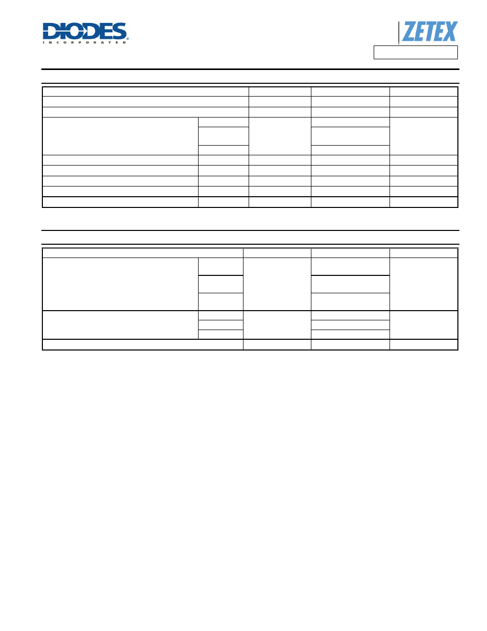
Maximum Ratings
(@T
A
= +25°C, unless otherwise specified.)
Characteristic Symbol
Value
Unit
Drain-Source Voltage
V
DSS
-60 V
Gate-Source Voltage
V
GS
20
V
Continuous Drain Current (V
GS
= 10V)
(Notes 7 & 9)
I
D
-4.8
A
T
A
= +70ºC
(Notes 7 & 9)
-3.8
(Notes 6 & 9)
-3.7
Pulsed Drain Current
(Notes 8)
I
DM
-23 A
Continuous Source Current (Body Diode)
(Notes 7)
I
S
-3.3 A
Pulsed Source Current (Body Diode)
(Notes 8)
I
SM
-23 A
Single Pulsed Avalanche Energy (L = 0.1mH)
(Note 11)
E
AS
38.2 mJ
Single Pulsed Avalanche Current (L = 0.1mH)
(Note 11)
I
AS
27.6 A
Thermal Characteristics
(@T
A
= +25°C, unless otherwise specified.)
Characteristic Symbol
Value
Unit
Power Dissipation
Linear Derating Factor
(Notes 6 & 9)
P
D
1.25
10
W
mW/°C
(Notes 6 & 10)
1.8
14
(Notes 7 & 9)
2.1
17
Thermal Resistance, Junction to Ambient
(Notes 6 & 9)
R
θJA
100
°C/W
(Notes 7 & 10)
69
(Notes 7 & 9)
58
Operating and Storage Temperature Range
T
J
, T
STG
-55 to +150
°C
Notes:
6. For a dual device surface mounted on 25mm x 25mm x 1.6mm FR4 PCB with a high coverage of single sided 1oz copper in still air conditions.
7. For a dual device surface mounted FR4 PCB measured at t
10 sec.
8. Repetitive rating 25mm x 25mm x 1.6mm FR4 PCB, D = 0.02, pulse width = 300µs – pulse width limited by maximum junction temperature.
9. For a dual device with one active die.
10. For a device with two active die running at equal power.
11. IAR and EAR rating are based on low frequency and duty cycles to keep T
J
= +25°C