Maximum ratings, Thermal characteristics – Diodes ZXMP6A17DN8 User Manual
Page 2
ZXMP6A17DN8
Document Number DS33588 Rev 4 - 2
2 of 8
August 2013
© Diodes Incorporated
ZXMP6A17DN8
ADVAN
CE I
N
F
O
RM
ATI
O
N
A Product Line of
Diodes Incorporated
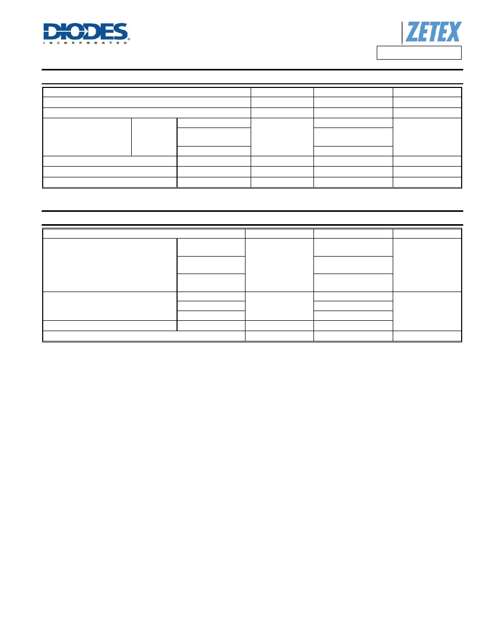
Maximum Ratings
(@T
A
= +25°C, unless otherwise specified.)
Characteristic Symbol
Value
Unit
Drain-Source voltage
V
DSS
-60 V
Gate-Source voltage
V
GS
20
V
Continuous Drain current
V
GS
= 10V
(Notes 7 & 9)
I
D
-3.42
A
T
A
= +70ºC
(Notes 7 & 9)
-2.73
(Notes 6 & 9)
-2.7
Pulsed Drain current
(Notes 8 & 9)
I
DM
-15.6 A
Continuous Source current (Body diode)
(Notes 7 & 9)
I
S
-3.4 A
Pulsed Source current (Body diode)
(Notes 8 & 9)
I
SM
-15.6 A
Thermal Characteristics
(@T
A
= +25°C, unless otherwise specified.)
Characteristic Symbol
Value
Unit
Power dissipation
Linear derating factor
(Notes 6 & 9)
P
D
1.25
10.0
W
mW/°C
(Notes 6 & 10)
1.81
14.5
(Notes 7 & 9)
2.15
17
Thermal Resistance, Junction to Ambient
(Notes 6 & 9)
R
θJA
100
°C/W
(Notes 6 & 10)
70
(Notes 7 & 9)
60
Thermal Resistance, Junction to Lead
(Notes 9 & 11)
R
θJL
51.68
Operating and storage temperature range
T
J
, T
STG
-55 to 150
°C
Notes:
6. For a device surface mounted on 25mm x 25mm x 1.6mm FR4 PCB with high coverage of single sided 1oz copper, in still air conditions; the device is
measured when operating in a steady-state condition.
7. Same as note (6), except the device is measured at t
10 sec.
8. Same as note (6), except the device is pulsed with D = 0.02 and pulse width 300µs. The pulse current is limited by the maximum junction temperature.
9. For a dual device with one active die.
10. For a device with two active die running at equal power.
11. Thermal resistance from junction to solder-point.