A dv a n ce i nf o rm at ion zxmn6a08e6, Maximum ratings, Thermal characteristics – Diodes ZXMN6A08E6 User Manual
Page 2
ZXMN6A08E6
Document Number DS33376 Rev. 7 - 2
2 of 8
December 2013
© Diodes Incorporated
A
DV
A
N
CE
I
NF
O
RM
AT
ION
ZXMN6A08E6
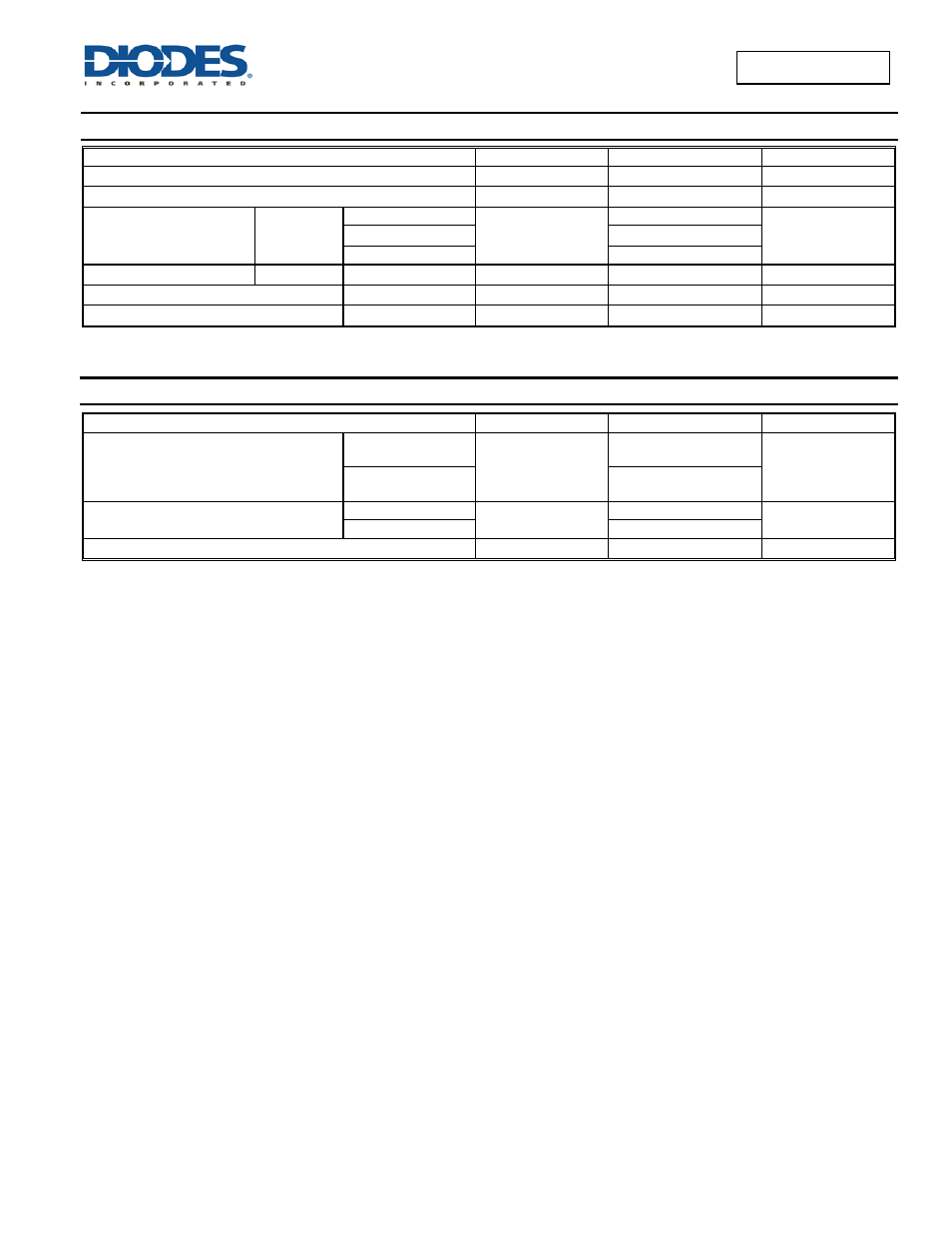
Maximum Ratings
(@T
A
= +25°C, unless otherwise specified.)
Characteristic
Symbol
Value
Unit
Drain-Source Voltage
V
DSS
60
V
Gate-Source Voltage
V
GS
±20
V
Continuous Drain Current
V
GS
= 10V
(Note 6)
I
D
3.5
A
T
A
= +70°C (Note 6)
2.8
(Note 5)
2.8
Pulsed Drain Current
V
GS
= 10V
(Note 7)
I
DM
16
A
Continuous Source Current (Body diode)
(Note 6)
I
S
2.6
A
Pulsed Source Current (Body diode)
(Note 7)
I
SM
16
A
Thermal Characteristics
(@T
A
= +25°C, unless otherwise specified.)
Characteristic
Symbol
Value
Unit
Power Dissipation
Linear Derating Factor
(Note 5)
P
D
1.1
8.8
W
mW/°C
(Note 6)
1.7
13.6
Thermal Resistance, Junction to Ambient
(Note 5)
R
θJA
113
°C/W
(Note 6)
73
Operating and Storage Temperature Range
T
J
, T
STG
-55 to +150
°C
Notes:
5. For a device surface mounted on 25mm x 25mm x 1.6mm FR4 PCB with high coverage of single sided 1oz copper, in still air conditions; the device is
measured when operating in a steady-state condition.
6. Same as note (5), except the device is measured at t
≤ 10 sec.
7. Same as note (5), except the device is pulsed with D = 0.02 and pulse width 300µs. The pulse current is limited by the maximum junction temperature.