Vn10lp, Maximum ratings, Thermal characteristics – Diodes VN10LP User Manual
Page 2
VN10LP
Document Number DS33198 Rev. 3 - 2
2 of 6
September 2012
© Diodes Incorporated
A Product Line of
Diodes Incorporated
VN10LP
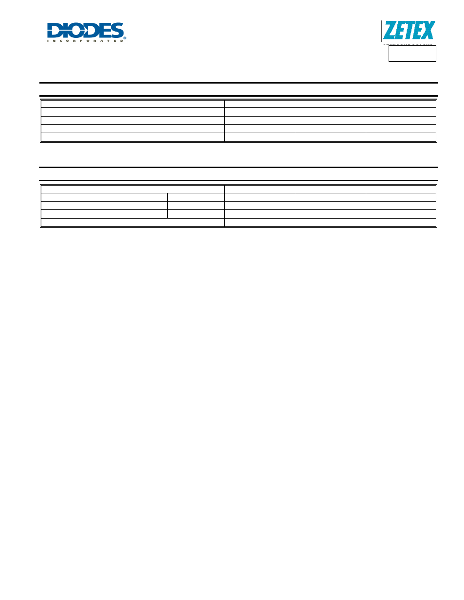
Maximum Ratings
(@T
A
= +25°C, unless otherwise specified.)
Characteristic
Symbol
Value
Unit
Drain-Source Voltage
V
DSS
60 V
Gate-Source Voltage
V
GSS
±20 V
Continuous Drain Current
I
D
270 mA
Pulsed Drain Current (Note 6)
I
DM
3 A
Thermal Characteristics
(@T
A
= +25°C, unless otherwise specified.)
Characteristic Symbol
Value
Unit
Power Dissipation
(Note 5)
P
D
625 mW
Thermal Resistance, Junction to Ambient
(Note 5)
R
θJA
200 °C/W
Thermal Resistance, Junction to Leads
(Note 7)
R
θJL
71 °C/W
Operating and Storage Temperature Range
T
J
,
T
STG
-55 to +150
°C
Notes:
5. For a device mounted on 25mm X 25mm X 1.6mm FR-4 PCB with high coverage of single sided 1oz copper, in still air condition.
6. Device mounted on minimum recommended pad layout test board, 10µs pulse duty cycle = 1%.
7. Thermal resistance from junction to Drain leads 2mm outside plastic compound.