Zxmn3a04k, Electrical characteristics (at t, 25°c unless otherwise stated) – Diodes ZXMN3A04K User Manual
Page 4
ZXMN3A04K
S E M I C O N D U C T O R S
ISSUE 1 - FEBRUARY 2004
4
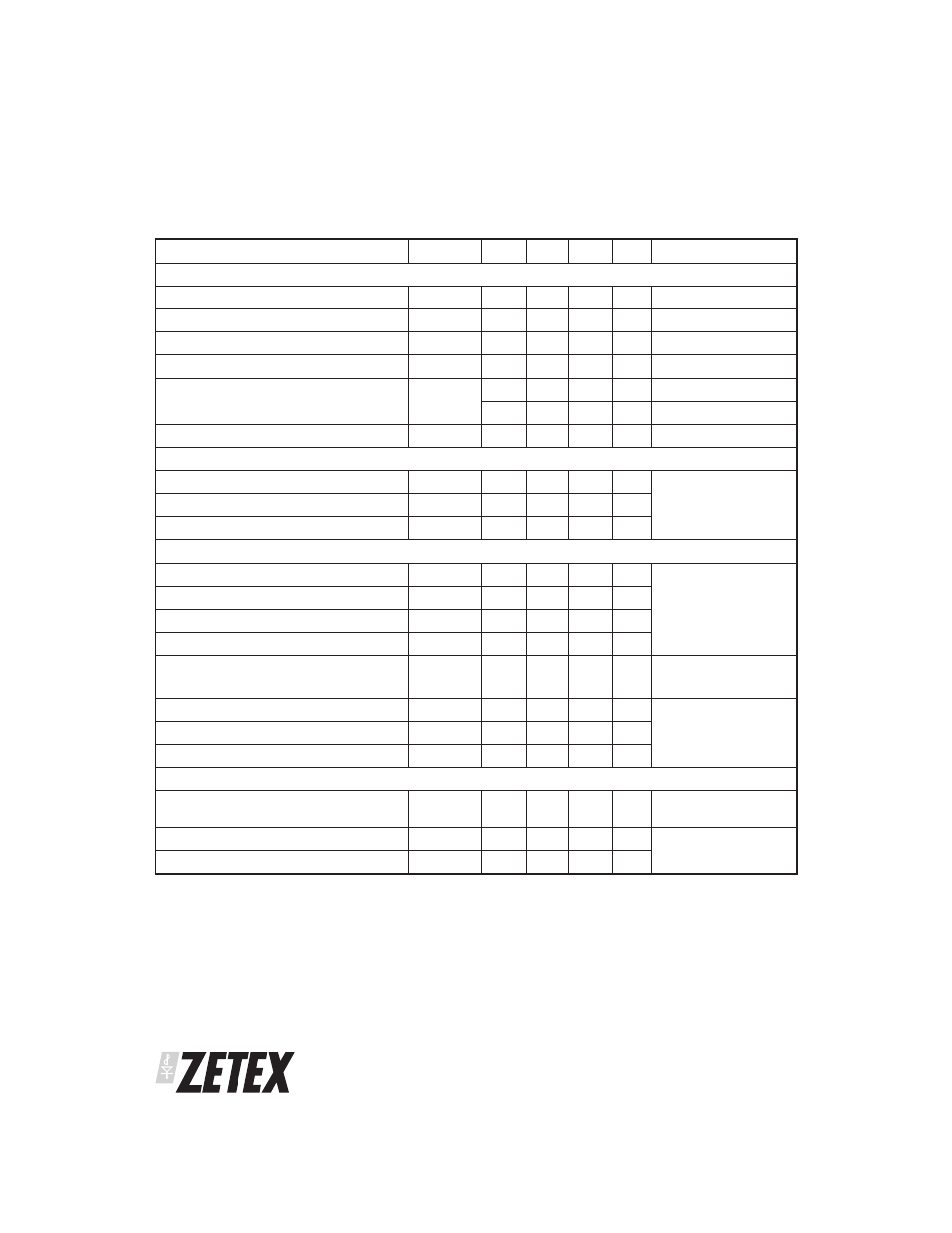
PARAMETER
SYMBOL
MIN.
TYP.
MAX.
UNIT CONDITIONS
STATIC
Drain-source breakdown voltage
V
(BR)DSS
30
V
I
D
= 250
A, V
GS
=0V
Zero gate voltage drain current
I
DSS
0.5
A V
DS
= 30V, V
GS
=0V
Gate-body leakage
I
GSS
100
nA
V
GS
=±20V, V
DS
=0V
Gate-source threshold voltage
V
GS(th)
1.0
V
I
D
= 250mA, V
DS
=V
GS
Static drain-source on-state resistance
(1)
R
DS(on)
0.02
⍀
V
GS
= 10V, I
D
= 12A
0.03
⍀
V
GS
= 4.5V, I
D
= 9.8A
Forward transconductance
(1) (3)
g
fs
22.1
S
V
DS
= 15V, I
D
= 12.6A
DYNAMIC
(3)
Input capacitance
C
iss
1890
pF
V
DS
= 15V, V
GS
=0V
f=1MHz
Output capacitance
C
oss
349
pF
Reverse transfer capacitance
C
rss
218
pF
SWITCHING
(2) (3)
Turn-on-delay time
t
d(on)
5.2
ns
V
DD
= 15V, I
D
= 1A
R
G
≅6.0⍀, V
GS
= 10V
Rise time
t
r
6.1
ns
Turn-off delay time
t
d(off)
38.1
ns
Fall time
t
f
20.2
ns
Total gate charge
Q
g
19.9
nC
V
DS
= 15V, V
GS
= 5V
I
D
= 6.5A
Total gate charge
Q
g
36.8
nC
V
DS
= 15V, V
GS
= 10V
I
D
= 6.5A
Gate-source charge
Q
gs
5.8
nC
Gate drain charge
Q
gd
7.1
nC
SOURCE-DRAIN DIODE
Diode forward voltage (1)
V
SD
0.85
0.95
V
T
j
=25°C, I
S
= 6.8A,
V
GS
=0V
Reverse recovery time (3)
t
rr
18.4
ns
T
j
=25°C, I
S
= 2.3A,
di/dt=100A/
s
Reverse recovery charge (3)
Q
rr
11
nC
ELECTRICAL CHARACTERISTICS (at T
amb
= 25°C unless otherwise stated)
NOTES
(1) Measured under pulsed conditions. Pulse width
Յ 300s; duty cycle Յ 2%.
(2) Switching characteristics are independent of operating junction temperature.
(3) For design aid only, not subject to production testing.