Electrical characteristics, Zxmd63n03x – Diodes ZXMD63N03X User Manual
Page 4
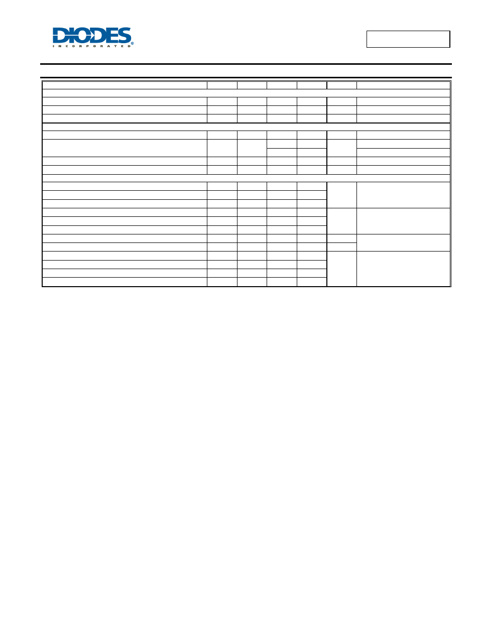
ZXMD63N03X
Document number: DS33501 Rev. 2 - 2
4 of 8
March 2014
© Diodes Incorporated
ZXMD63N03X
Electrical Characteristics
(@T
A
= +25°C, unless otherwise specified.)
Characteristic
Symbol
Min
Typ
Max
Unit
Test Condition
OFF CHARACTERISTICS
Drain-Source Breakdown Voltage
BV
DSS
30 —
— V
V
GS
= 0V, I
D
= 250μA
Zero Gate Voltage Drain Current T
J
= +25°C
I
DSS
—
—
1.0 µA
V
DS
= 30V, V
GS
= 0V
Gate-Source Leakage
I
GSS
—
—
100 nA
V
GS
= ±20V, V
DS
= 0V
ON CHARACTERISTICS
Gate Threshold Voltage
V
GS(th)
1.0 —
—
V
V
DS
= V
GS
, I
D
= 250μA
Static Drain-Source On-Resistance (Note 11)
R
DS (ON)
—
—
135
mΩ
V
GS
= 10V, I
D
= 1.7A
—
200
V
GS
= 4.5V, I
D
= 0.85A
Forward Transconductance (Notes 11 & 13)
g
fs
1.9 —
— S
V
DS
= 10V, I
D
= 0.85A
Diodes Forward Voltage (Note 11)
V
SD
— —
0.95 V
T
J
= 25°C, I
S
= 1.7A, V
GS
= 0V
DYNAMIC CHARACTERISTICS
Input Capacitance (Note 12 & 13)
C
iss
—
290 —
pF
V
DS
= 25V, V
GS
= 0V,
f = 1.0MHz
Output Capacitance (Notes 12 & 13)
C
oss
—
70 —
Reverse Transfer Capacitance (Notes 12 & 13)
C
rss
—
20 —
Total Gate Charge (Notes 12 & 13)
Q
g
—
—
8
nC
V
GS
= 10V, V
DS
= 24V,
I
D
= 1.7A
Gate-Source Charge (Notes 12 & 13)
Q
gs
—
—
1.2
Gate-Drain Charge (Notes 12 & 13)
Q
gd
—
—
2
Reverse Recovery Time (Note 13)
t
rr
—
16.9 —
ns
T
J
= +25°C, I
F
= 1.7A,
di/dt = 100A/µs
Reverse Recovery Charge (Note 13)
Q
rr
—
9.5 —
nC
Turn-On Delay Time (Notes 12 & 13)
t
D(on)
—
2.5 —
ns
V
DD
= 15V, I
D
= 1.7A,
R
G
= 6.1Ω, R
D
= 8.7Ω,
Turn-On Rise Time (Notes 12 & 13)
t
r
—
4.1 —
Turn-Off Delay Time (Notes 12 & 13)
t
D(off)
—
9.6 —
Turn-Off Fall Time (Notes 12 & 13)
t
f
—
4.4 —
Notes:
11. Measured under pulsed conditions. Pulse width
300s; duty cycle 2%.
12. Switching characteristics are independent of operating junction temperature.
13. For design aid only, not subject to production testing.