Zxmd63n03x, Maximum ratings, Thermal characteristics – Diodes ZXMD63N03X User Manual
Page 2
ZXMD63N03X
Document number: DS33501 Rev. 2 - 2
2 of 8
March 2014
© Diodes Incorporated
ZXMD63N03X
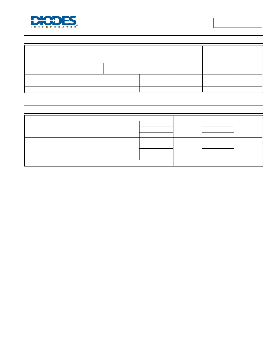
Maximum Ratings
(@T
A
= +25°C, unless otherwise specified.)
Characteristic
Symbol
Value
Unit
Drain-Source Voltage
V
DSS
30 V
Gate-Source Voltage
V
GSS
±20 V
Continuous Drain Current
Steady
State
@ V
GS
= 4.5V; T
A
= +25°C (Note 5 & 6)
@ V
GS
= 4.5V;
T
A
= +70°C (Note 5 & 6)
I
D
2.3
1.8
A
Pulsed Drain Current
(Notes 6 & 7)
I
DM
14 A
Continuous Source Current (Body Diode)
(Notes 5 & 6)
I
S
1.5 A
Pulsed Source Current (Body Diode)
(Notes 6 & 7)
I
SM
14 A
Thermal Characteristics
Characteristic Symbol
Value
Unit
Power Dissipation
(Notes 6 & 8)
P
D
0.87
W
(Notes 5 & 6)
1.25
(Notes 8 & 9)
1.04
Thermal Resistance, Junction to Ambient
(Notes 6 & 8)
R
θJA
143
°C/W
(Notes 5 & 6)
100
(Notes 8 & 9)
120
Thermal Resistance, Junction to Leads
(Note 10)
R
θJL
84.9 °C/W
Operating and Storage Temperature Range
T
J
,
T
STG
-55 to +150
°C
Notes:
5. For a device surface mounted on FR4 PCB measured at t
10 sec.
6. For device with one active die.
7. Repetitive rating - 25mm x 25mm FR4 PCB, D = 0.02, pulse width 300μs – pulse width limited by maximum junction temperature.
8. For a device surface mounted on 25mm x 25mm FR4 PCB with high coverage of single sided 1oz copper, in still air conditions.
9. For device with two active die running at equal power.
10. Thermal resistance from junction to solder-point (at the end of the drain lead).