Zxm61n03f, Absolute maximum ratings, Thermal resistance – Diodes ZXM61N03F User Manual
Page 2
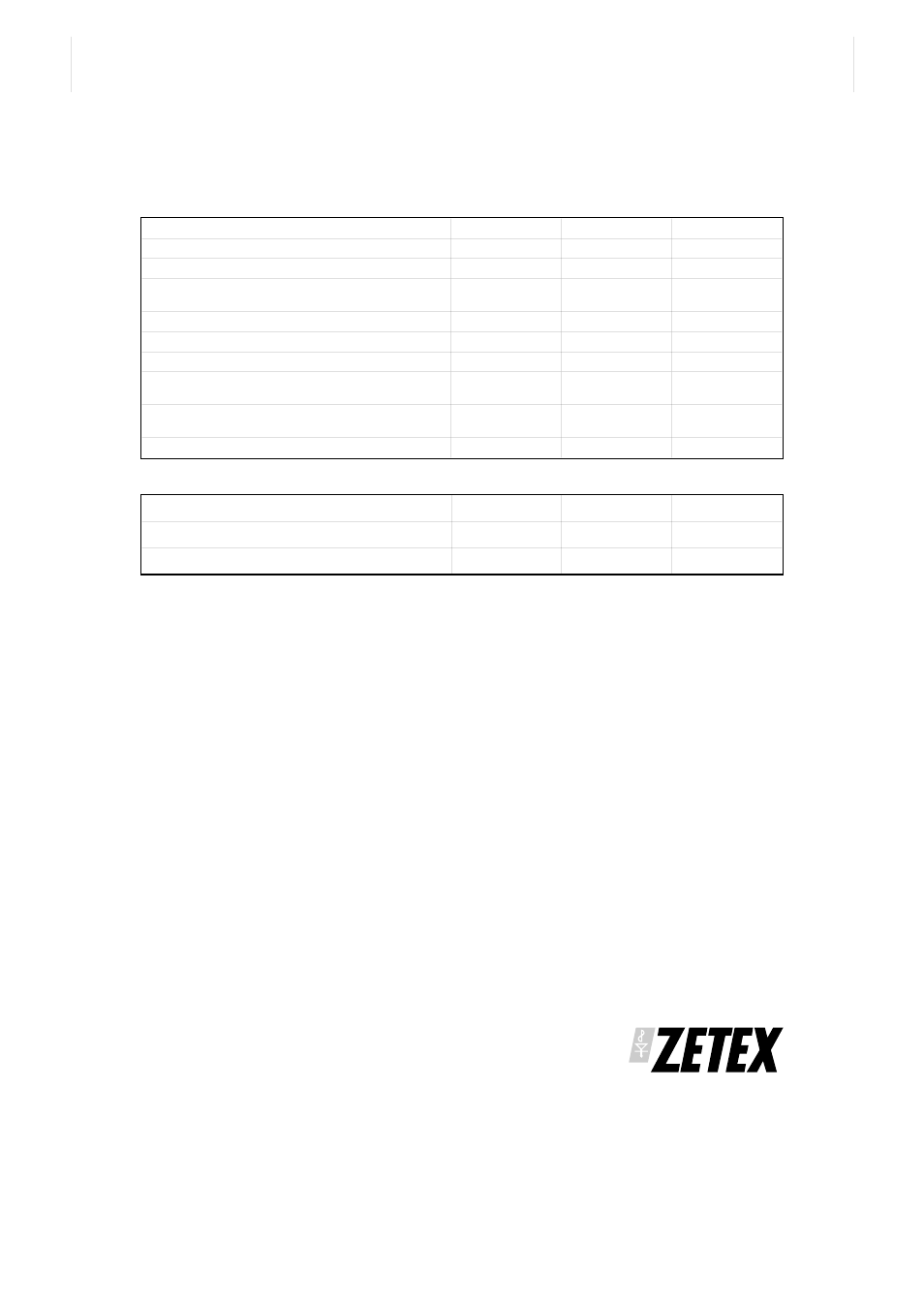
ZXM61N03F
ABSOLUTE MAXIMUM RATINGS.
PARAMETER
SYMBOL
LIMIT
UNIT
Drain-Source Voltage
V
DSS
30
V
Gate Source Voltage
V
GS
±
20
V
Continuous Drain Current (V
GS
=10V; T
A
=25°C)(b)
(V
GS
=10V; T
A
=70°C)(b)
I
D
1.4
1.1
A
Pulsed Drain Current (c)
I
DM
7.3
A
Continuous Source Current (Body Diode) (b)
I
S
0.8
A
Pulsed Source Current (Body Diode)
I
SM
7.3
A
Power Dissipation at T
A
=25°C (a)
Linear Derating Factor
P
D
625
5
mW
mW/°C
Power Dissipation at T
A
=25°C (b)
Linear Derating Factor
P
D
806
6.4
mW
mW/°C
Operating and Storage Temperature Range
T
j
:T
stg
-55 to +150
°C
THERMAL RESISTANCE
PARAMETER
SYMBOL
VALUE
UNIT
Junction to Ambient (a)
R
θ
JA
200
°C/W
Junction to Ambient (b)
R
θ
JA
155
°C/W
NOTES
(a) For a device surface mounted on 25mm x 25mm FR4 PCB with high coverage of single sided 1oz copper,
in still air conditions
(b) For a device surface mounted on FR4 PCB measured at t
р5 secs.
(c) Repetitive rating - pulse width limited by maximum junction temperature. Refer to Transient Thermal
Impedance graph.
2
ISSUE
1 - JUNE 2004