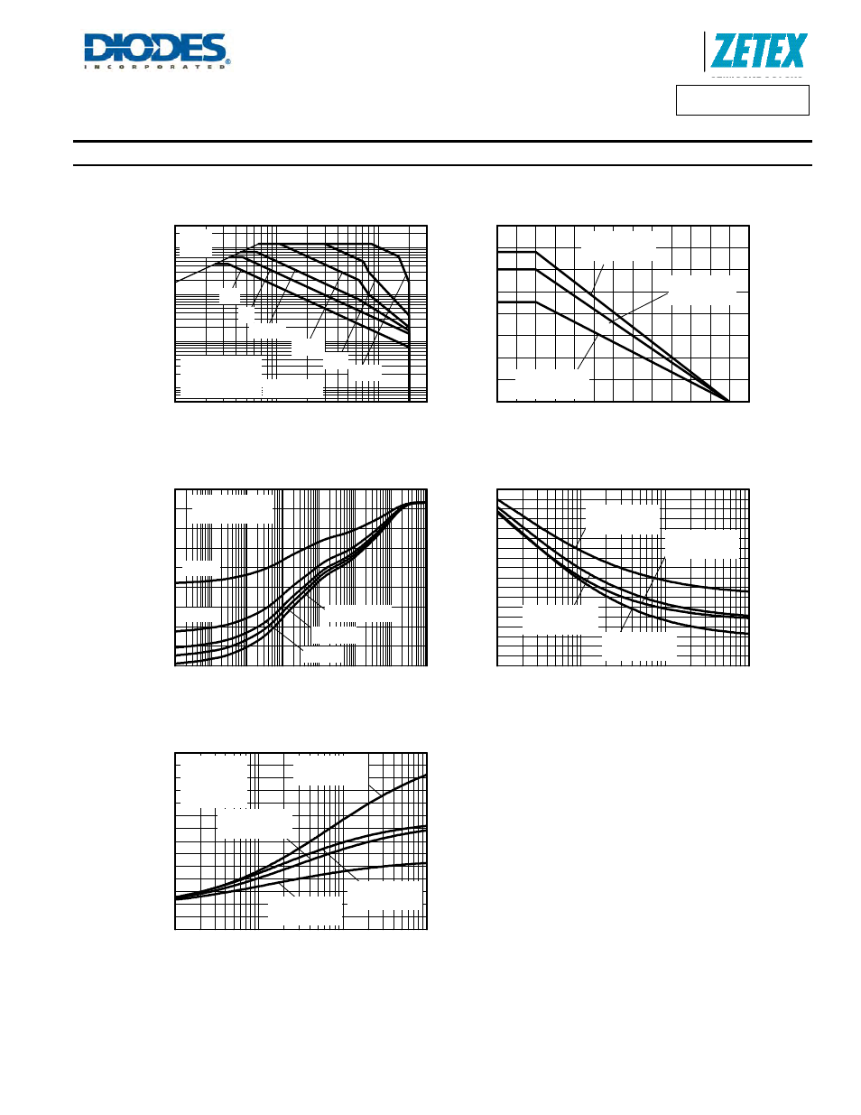
Zxtns618mc, Npn - thermal characteristics, Safe operating area – Diodes ZXTNS618MC User Manual
Page 3: Derating curve, Transient thermal impedance, Thermal resistance v board area, Power dissipation v board area
ZXTNS618MC
Document Number DS31933 Rev. 4 - 2
3 of 10
June 2011
© Diodes Incorporated
A Product Line of
Diodes Incorporated
ZXTNS618MC
NPN - Thermal Characteristics
0.1
1
10
0.01
0.1
1
10
0
25
50
75
100
125
150
0.0
0.5
1.0
1.5
2.0
100µ
1m
10m 100m
1
10
100
1k
0
20
40
60
80
0.1
1
10
100
0
25
50
75
100
125
150
175
200
225
0.1
1
10
100
0.0
0.5
1.0
1.5
2.0
2.5
3.0
3.5
8sqcm 2oz Cu
One active die
Single Pulse
100us
100ms
1s
V
CE(SAT)
Limited
1ms
Safe Operating Area
T
amb
=25°C
DC
10ms
I
C
Co
lle
c
to
r Cu
rre
n
t (A
)
V
CE
Collector-Emitter Voltage (V)
1 0 s q c m 1 o z C u
O n e a c t i v e d i e
8 s q c m 2 o z C u
O n e a c t i v e d i e
1 0 s q c m 1 o z C u
T w o a c t i v e d i e
Derating Curve
M
a
x P
o
we
r Di
ssi
p
a
ti
o
n
(W
)
Temperature (°C)
8sqcm 2oz Cu
One active die
D=0.2
D=0.5
D=0.1
Transient Thermal Impedance
Single Pulse
D=0.05
Th
er
m
a
l R
e
si
st
a
n
c
e (
°C
/W
)
Pulse Width (s)
1oz copper
Two active die
1oz copper
One active die
2oz copper
One active die
2oz copper
Two active die
Thermal Resistance v Board Area
Th
er
m
a
l R
e
si
st
a
n
c
e (
°C
/W
)
Board Cu Area (sqcm)
1oz copper
Two active die
2oz copper
Two active die
1oz copper
One active die
2oz copper
One active die
Power Dissipation v Board Area
T
amb
=25°C
T
j max
=150°C
Continuous
P
D
Di
ssi
p
a
ti
o
n
(W
)
Board Cu Area (sqcm)