Maximum ratings, pre-biased npn transistor, q, Maximum ratings, pre-biased pnp transistor, q, Thermal characteristics – Diodes UMC5N User Manual
Page 2: Umc5n
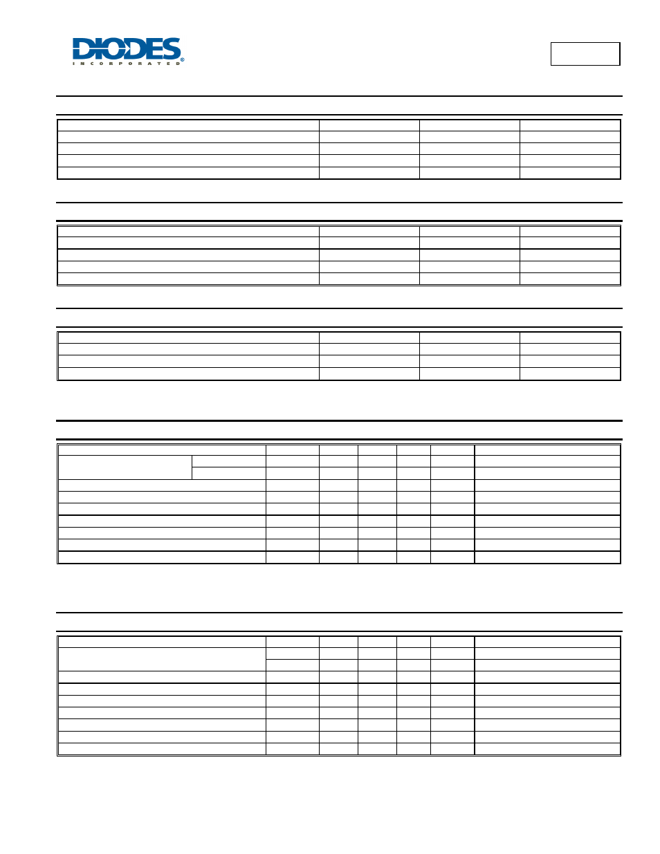
UMC5N
Document number: DS31205 Rev. 4 - 2
2 of 5
November 2011
© Diodes Incorporated
UMC5N
Maximum Ratings, Pre-Biased NPN Transistor, Q
1
@T
A
= 25°C unless otherwise specified
Characteristic Symbol
Value
Unit
Supply Voltage
V
CC
50 V
Input Voltage
V
IN
-10 to +40
V
Output Current
I
O
30 mA
Collector Current
I
C(MAX)
100 mA
Maximum Ratings, Pre-Biased PNP Transistor, Q
2
@T
A
= 25°C unless otherwise specified
Characteristic Symbol
Value
Unit
Supply Voltage
V
CC
-50 V
Input Voltage
V
IN
-20 to +7
V
Output Current
I
O
-100 mA
Collector Current
I
C(MAX)
-100 mA
Thermal Characteristics
Characteristic Symbol
Value
Unit
Power Dissipation (Note 4)
P
D
150 mW
Thermal Resistance, Junction to Ambient Air (Note 4)
R
θJA
833
°C/W
Operating and Storage Temperature Range
T
J
, T
STG
-55 to +150
°C
Notes:
4. Device mounted on FR-4 PCB; pad layout as shown on Diodes Inc. suggested pad layout document AP02001, which can be found on our website at
Electrical Characteristics, Pre-Biased NPN Transistor, Q
1
@T
A
= 25°C unless otherwise specified
Characteristic Symbol
Min
Typ
Max
Unit
Test
Condition
Input Voltage
(Note 5)
V
I(OFF)
0.5
⎯
⎯
V
V
CC
= 5V, I
O
= 100
μA
(Note 6)
V
I(ON)
⎯
⎯
3 V
V
O
= 0.3V, I
O
= 2mA
Output Voltage
V
O(ON)
⎯
0.1 0.3 V I
O
/ I
I
= 10mA/0.5 mA
Input Current
I
I
⎯
⎯
0.18 mA
V
I
= 5V
Output Current
I
O(OFF)
⎯
⎯
0.5
μA
V
CC
= 50V, V
I
= 0V
DC Current Gain
G
I
68
⎯
⎯
⎯
V
O
= 5V, I
O
= 5mA
Gain-Bandwidth Product (Note 7)
f
T
⎯
250
⎯
MHz
V
CE
= 10V, I
E
= -5mA, f = 100MHz
Input Resistance
R
1
32.9 47 61.1 k
Ω
⎯
Resistance Ratio
R
2
/R
1
0.8 1 1.2
⎯
⎯
Notes:
5. The device is guaranteed to be in “OFF” state with V
I(OFF)
up to 0.5V
6. The device is guaranteed to be in “ON” state with V
I(ON)
starting from 3V
7. Characteristic of Transistor – for reference only.
Electrical Characteristics, Pre-Biased PNP Transistor, Q
2
@T
A
= 25°C unless otherwise specified
Characteristic Symbol
Min
Typ
Max
Unit
Test
Condition
Input Voltage
V
I(OFF)
-0.3
⎯
⎯
V
V
CC
= -5V, I
O
= -100
μA
V
I(ON)
⎯
⎯
-2.5 V
V
O
= -0.3V, I
O
= -20mA
Output Voltage
V
O(ON)
⎯
-0.1 -0.3 V I
O
/ I
I
= -10mA/-0.5 mA
Input Current
I
I
⎯
⎯
-1.8 mA
V
I
= -5V
Output Current
I
O(OFF)
⎯
⎯
-0.5
μA
V
CC
= -50V, V
I
= 0V
DC Current Gain
G
I
30
⎯
⎯
⎯
V
O
= -5V, I
O
= -10mA
Gain-Bandwidth Product (Note 7)
f
T
⎯
250
⎯
MHz
V
CE
= -10V, I
E
= 5mA, f = 100MHz
Input Resistance
R
1
3.29 4.7 6.11 k
Ω
⎯
Resistance Ratio
R
2
/R
1
1.7 2.1 2.6
⎯
⎯
Notes:
8. The device is guaranteed to be in “OFF” state with V
I(OFF)
up to -0.3V
9. The device is guaranteed to be in “ON” state with V
I(ON)
starting from -2.5V
10. Characteristic of Transistor – for reference only.