Zxtn4004k, Maximum ratings, Thermal characteristics – Diodes ZXTN4004K User Manual
Page 2: Thermal characteristics and derating information, Derating curve, Transient thermal impedance, Pulse power dissipation
ZXTN4004K
Document Number: DS35458 Rev: 1 - 2
2 of 5
December 2011
© Diodes Incorporated
A Product Line of
Diodes Incorporated
ZXTN4004K
Maximum Ratings
@T
A
= 25°C unless otherwise specified
Characteristic Symbol
Value
Unit
Collector-Base Voltage
V
CBO
150 V
Collector-Emitter Voltage
V
CEO
150 V
Emitter-Base Voltage
V
EBO
7 V
Continuous Collector Current
I
C
1 A
Peak Pulse Current (Note 4)
I
CM
3 A
Base Current
I
B
500 mA
Thermal Characteristics
@T
A
= 25°C unless otherwise specified
Characteristic Symbol
Value
Unit
Power Dissipation
(Note 3)
P
D
3.8 W
Thermal Resistance, Junction to Ambient
(Note 3)
R
θJA
33
°C/W
Thermal Resistance, Junction to Leads
(Note 5)
R
θJL
12
°C/W
Operating and Storage Temperature Range
T
J,
T
STG
-55 to +150
°C
Notes:
3. For a device surface mounted on 50mm X 50mm FR4 PCB with high coverage of single sided 2 oz copper, in still air conditions
4. Measured under pulsed conditions. Pulse width = 300µs. Duty cycle
≤ 2%.
5. Thermal resistance from junction to solder-point (on the exposed collector pad).
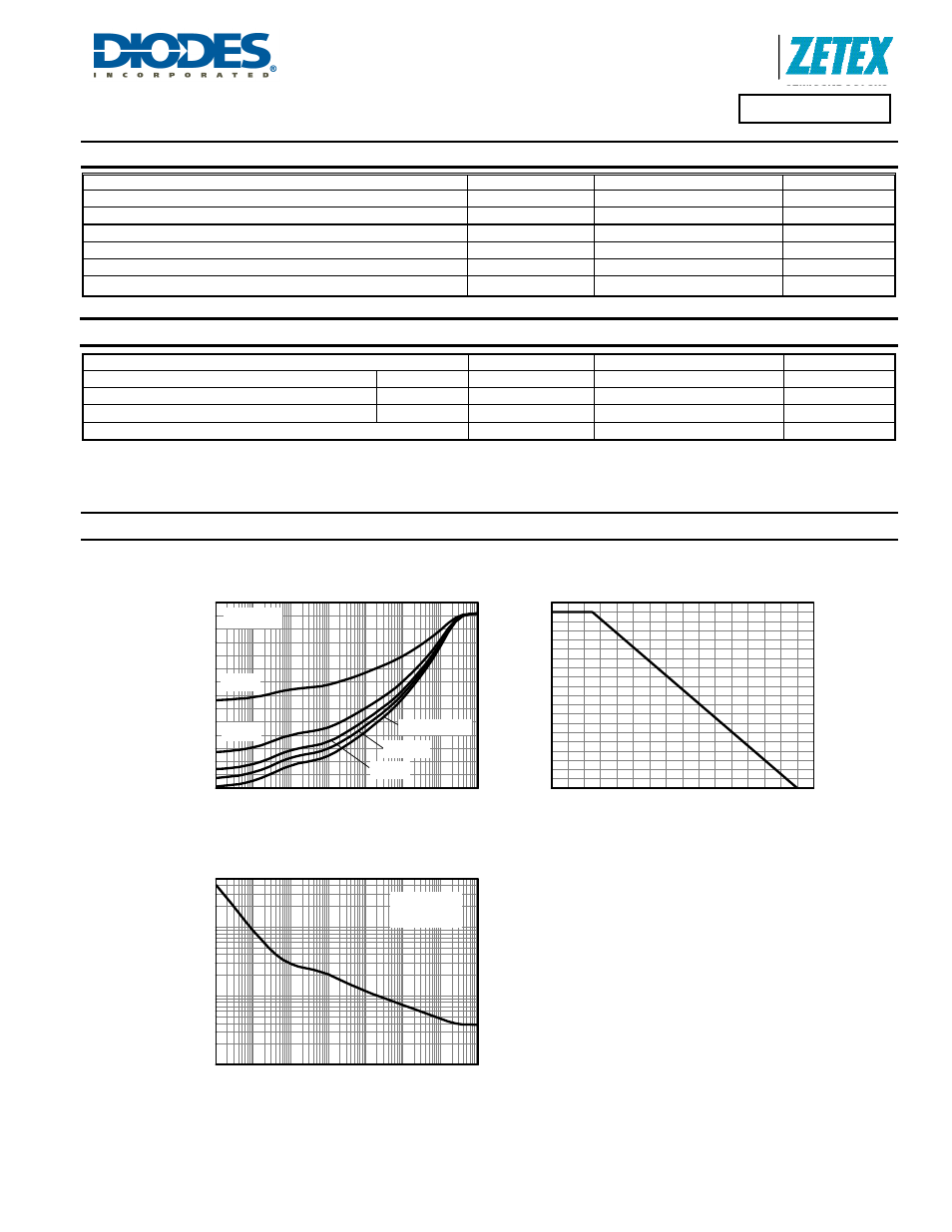
Thermal Characteristics and Derating Information
0
20
40
60
80
100
120
140
160
0.0
0.4
0.8
1.2
1.6
2.0
2.4
2.8
3.2
3.6
4.0
Derating Curve
Temperature (°C)
M
a
x P
o
wer Di
s
s
ip
at
io
n (W)
100µ
1m
10m 100m
1
10
100
1k
0
5
10
15
20
25
30
35
T
amb
=25°C
Transient Thermal Impedance
D=0.5
D=0.2
D=0.1
Single Pulse
D=0.05
T
herm
a
l Resist
ance (°
C/
W)
Pulse Width (s)
100µ
1m
10m 100m
1
10
100
1k
1
10
100
Single Pulse
T
amb
=25°C
Pulse Power Dissipation
Pulse Width (s)
Ma
x
im
u
m Po
w
e
r (
W
)