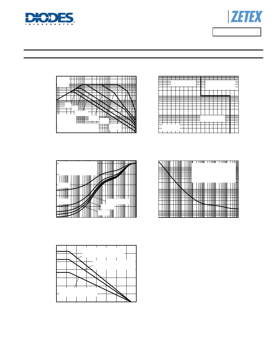
Thermal characteristics and derating information, Safe operating area, Derating curve – Diodes ZXTN25100BFH User Manual
Page 3: Transient thermal impedance, Pulse power dissipation
ZXTN25100BFH
Document number: DS33703 Rev. 2 - 2
3 of 7
December 2012
© Diodes Incorporated
A Product Line of
Diodes Incorporated
ZXTN25100BFH
Thermal Characteristics and Derating information
0
20 40 60 80 100 120 140 160 180
1µ
10µ
100µ
100m
1
10
100
10m
100m
1
10
Safe Operating Area
50mm X 50mm X 1.6mm FR4
2oz Cu
Single Pulse
T
amb
=25°C
V
CE(sat)
Limited
100µs
1ms
10ms
100ms
1s
DC
Safe Operating Area
I
C
Col
le
ct
or Curre
nt
(A
)
V
CE
Collector-Emitter Voltage (V)
0
20
40
60
80
100 120 140 160
0.0
0.2
0.4
0.6
0.8
1.0
1.2
1.4
25mm X 25mm X 1.6mm FR4
2oz Cu
15mm X 15mm X 1.6mm FR4
1oz Cu
Derating Curve
Temperature (°C)
M
a
x P
o
wer Di
ss
ip
at
io
n
(W)
50mm X 50mm X 1.6mm FR4
2oz Cu
100µ
1m
10m 100m
1
10
100
1k
0
20
40
60
80
100
T
amb
=25°C
50mm X 50mm X 1.6mm FR4
2oz Cu
Transient Thermal Impedance
D=0.5
D=0.2
D=0.1
Single Pulse
D=0.05
T
h
e
rm
a
l Re
si
st
a
nce
(
°C/
W
)
Pulse Width (s)
100µ
1m
10m 100m
1
10
100
1k
1
10
100
Single Pulse
T
amb
=25°C
50mm X 50mm X 1.6mm FR4
2oz Cu
Pulse Power Dissipation
Pulse Width (s)
Max
imum P
ow
e
r (
W
)
BV
(BR)CEV
=170V
BV
(BR)CEO
=100V
Failure may occur
in this region
T
amb
=25°C
V
CE
Collector-Emitter Voltage (V)
I
C
Co
lle
ct
or Current
(A
)