Zxtp2009z – Diodes ZXTP2009Z User Manual
Page 2
ZXTP2009Z
S E M I C O N D U C T O R S
ISSUE 1 - JUNE 2005
2
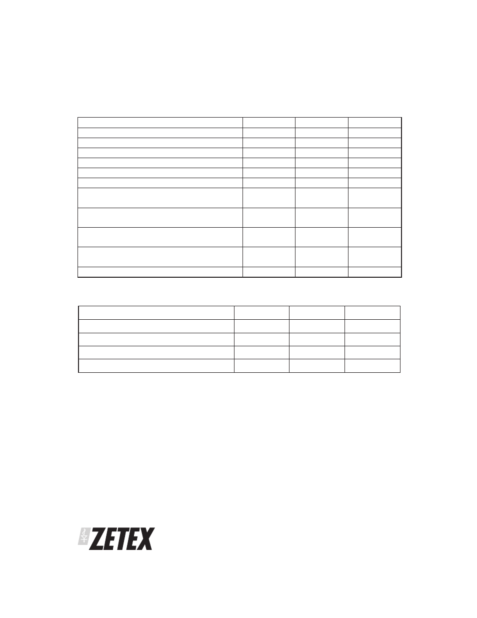
PARAMETER
SYMBOL
VALUE
UNIT
Junction to ambient
(a)
R
⍜JA
139
°C/W
Junction to ambient
(b)
R
⍜JA
83
°C/W
Junction to ambient
(c)
R
⍜JA
60
°C/W
Junction to ambient
(d)
R
⍜JA
42
°C/W
NOTES
(a) For a device surface mounted on 15mm x 15mm x 1.6mm FR4 PCB with high coverage of single sided 1oz copper, in still air conditions.
(b) For a device surface mounted on 25mm x 25mm x 1.6mm FR4 PCB with high coverage of single sided 1oz copper, in still air conditions.
(c) For a device surface mounted on 50mm x 50mm x 1.6mm FR4 PCB with high coverage of single sided 1oz copper, in still air conditions.
(d) For a device surface mounted on 25mm x 25mm x 1.6mm FR4 PCB measured at t
Ͻ 5 secs.
THERMAL RESISTANCE
PARAMETER
SYMBOL
LIMIT
UNIT
Collector-base voltage
BV
CBO
-50
V
Collector-base voltage
BV
CBS
-50
V
Collector-emitter voltage
BV
CEO
-40
V
Emitter-base voltage
BV
EBO
-7.5
V
Continuous collector current
(b)
I
C
-5.5
A
Peak pulse current
I
CM
-15
A
Power dissipation at T
A
=25°C
(a)
Linear derating factor
P
D
0.9
7.2
W
mW/°C
Power dissipation at T
A
=25°C
(b)
Linear derating factor
P
D
1.5
12
W
mW/°C
Power dissipation at T
A
=25°C
(c)
Linear derating factor
P
D
2.1
16.8
W
mW/°C
Power dissipation at T
A
=25°C
(d)
Linear derating factor
P
D
3
24
W
mW/°C
Operating and storage temperature range
T
j
, T
stg
-55 to 150
°C
ABSOLUTE MAXIMUM RATINGS