Zxtn2040f, Maximum ratings, Thermal characteristics – Diodes ZXTN2040F User Manual
Page 2: Derating curve, Transient thermal impedance, Pulse power dissipation
ZXTN2040F
Document number: DS33668 Rev. 3 - 2
2 of 6
August 2012
© Diodes Incorporated
ZXTN2040F
A Product Line of
Diodes Incorporated
Maximum Ratings
(@T
A
= +25°C, unless otherwise specified.)
Characteristic Symbol
Value
Unit
Collector-Base Voltage
V
CBO
40 V
Collector-Emitter Voltage
V
CEO
40 V
Emitter-Base Voltage
V
EBO
6 V
Continuous Collector Current (Note 5)
I
C
1 A
Peak Pulse Current
I
CM
2 A
Peak Base Current
I
BM
1 A
Thermal Characteristics
Characteristic Symbol
Value
Unit
Collector Power Dissipation
(Note 5)
P
D
310
mW
(Note 6)
350
Thermal Resistance, Junction to Ambient
(Note 5)
R
θJA
403
°C/W
(Note 6)
357
Thermal Resistance, Junction to Leads
(Note 7)
R
θJL
350
°C/W
Operating and Storage Temperature Range
T
J,
T
STG
-55 to +150
°C
Notes:
5. For the device mounted on minimum recommended pad layout FR4 PCB with high coverage of single sided 1oz copper in still air condition.
6. Same as Note 5, expect the device is mounted on 15mm X 15mm X 1.6mm FR4 PCB.
7. Thermal resistance from junction to solder-point (at the end of the collector lead).
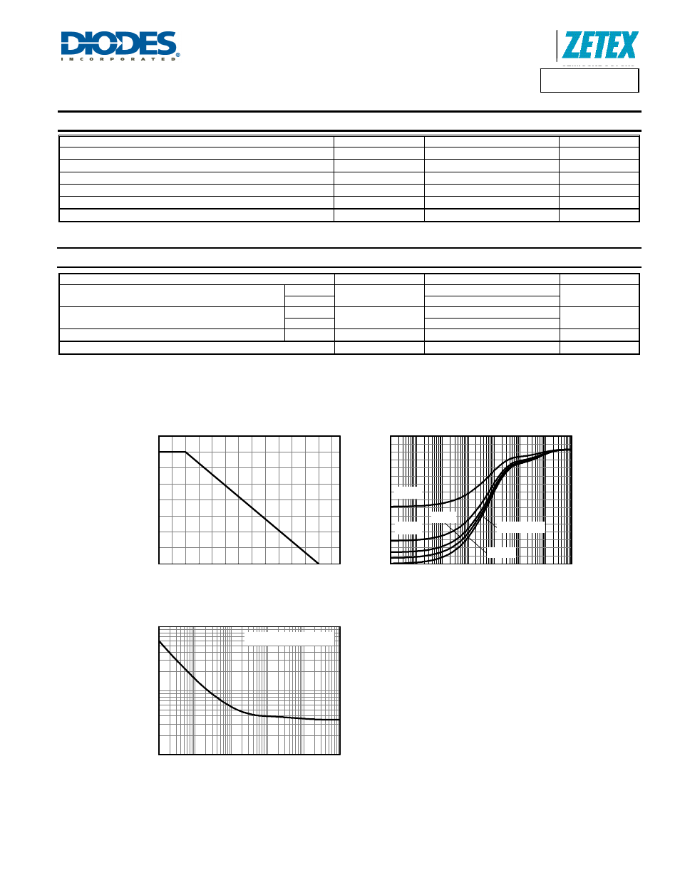
0
25
50
75
100
125
150
0.0
0.1
0.2
0.3
0.4
Derating Curve
Temperature (°C)
M
a
x
P
o
we
r Di
ssi
p
a
ti
o
n
(W)
100µ
1m
10m 100m
1
10
100
1k
0
50
100
150
200
250
300
350
400
Transient Thermal Impedance
D=0.5
D=0.2
D=0.1
Single Pulse
D=0.05
T
h
erm
al
Resist
ance (°
C/
W)
Pulse Width (s)
10m
100m
1
10
100
1k
0.1
1
10
Single Pulse. T
amb
=25°C
Pulse Power Dissipation
Pulse Width (s)
M
a
x
P
o
wer
Diss
ip
at
io
n (W)