Zxt12p40dx, Package dimensions pad layout details, Conforms to jedec mo-187 iss a – Diodes ZXT12P40DX User Manual
Page 6
Europe
Zetex GmbH
Kustermann-park
Balanstraße 59
D-81541 München
Germany
Telefon: (49) 89 45 49 49 0
Fax: (49) 89 45 49 49 49
[email protected]
Americas
Zetex Inc
700 Veterans Memorial Highway
Hauppauge, NY 11788
USA
Telephone: (1) 631 360 2222
Fax: (1) 631 360 8222
[email protected]
Asia Pacific
Zetex (Asia Ltd)
3701-04 Metroplaza Tower 1
Hing Fong Road, Kwai Fong
Hong Kong
Telephone: (852) 26100 611
Fax: (852) 24250 494
[email protected]
Corporate Headquarters
Zetex Semiconductors plc
Zetex Technology Park, Chadderton
Oldham, OL9 9LL
United Kingdom
Telephone (44) 161 622 4444
Fax: (44) 161 622 4446
[email protected]
© 2006 Published by Zetex Semiconductors plc.
ISSUE
2 - DECEMBER 2006
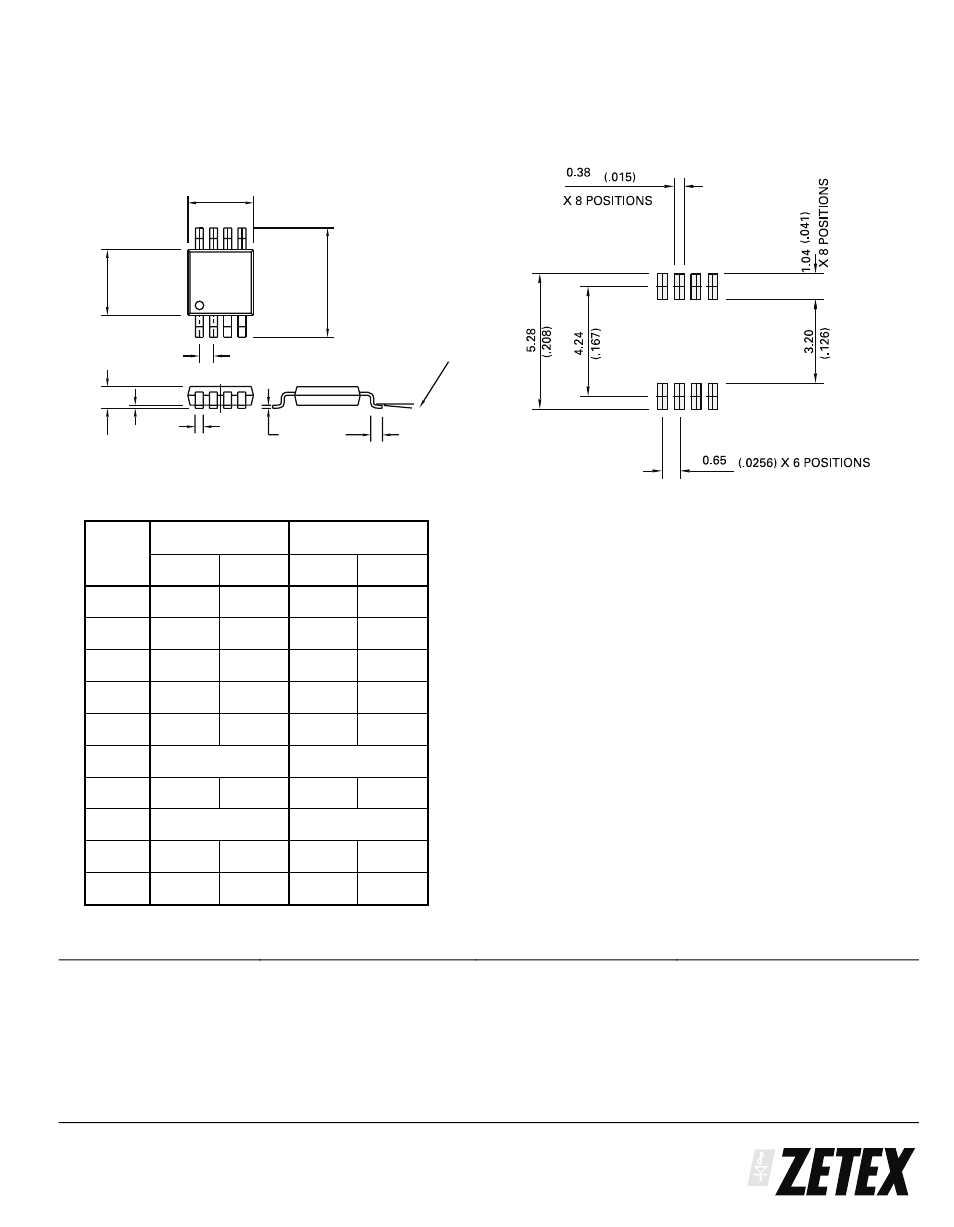
ZXT12P40DX
PACKAGE DIMENSIONS
PAD LAYOUT DETAILS
6
H
E
D
e X 6
A1
L
C
1
2
3
4
5
6
7
8
θ°
B
Conforms to JEDEC MO-187 Iss A
DIM
Millimetres
Inches
MIN
MAX
MIN
MAX
A
1.10
0.043
A1
0.05
0.15
0.002
0.006
B
0.25
0.40
0.010
0.016
C
0.13
0.23
0.005
0.009
D
2.90
3.10
0.114
0.122
e
0.65
BSC
0.0256
BSC
E
2.90
3.10
0.114
0.122
H
4.90
BSC
0.193
BSC
L
0.40
0.70
0.016
0.028
q°
0°
6°
0°
6°