Zxt12n20dx – Diodes ZXT12N20DX User Manual
Page 2
ISSUE 1 - MARCH 2000
ZXT12N20DX
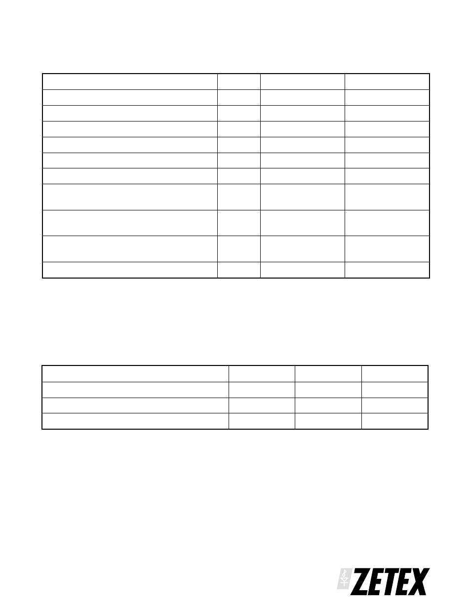
THERMAL RESISTANCE
PARAMETER
SYMBOL
VALUE
UNIT
Junction to Ambient (a)(d)
R
θ
JA
143
°C/W
Junction to Ambient (b)(d)
R
θ
JA
100
°C/W
Junction to Ambient (a)(e)
R
θ
JA
120
°C/W
NOTES
(a) For a device surface mounted on 25mm x 25mm FR4 PCB with high coverage of single sided 1oz copper,
in still air conditions
(b) For a device surface mounted on FR4 PCB measured at t
р5 secs.
(c) Repetitive rating - pulse width limited by maximum junction temperature. Refer to Transient Thermal
Impedance graph.
(d) For device with one active die.
(e) For device with two active die running at equal power.
2
ABSOLUTE MAXIMUM RATINGS.
PARAMETER
SYMBOL
LIMIT
UNIT
Collector-Base Voltage
V
CBO
50
V
Collector-Emitter Voltage
V
CEO
20
V
Emitter-Base Voltage
V
EBO
7.5
V
Peak Pulse Current
I
CM
15
A
Continuous Collector Current
I
C
3.5
A
Base Current
I
B
500
mA
Power Dissipation at TA=25°C (a)(d)
Linear Derating Factor
P
D
0.87
6.9
W
mW/°C
Power Dissipation at TA=25°C (a)(e)
Linear Derating Factor
P
D
1.04
8.3
W
mW/°C
Power Dissipation at TA=25°C (b)(d)
Linear Derating Factor
P
D
1.25
10
W
mW/°C
Operating and Storage Temperature Range
T
j
:T
stg
-55 to +150
°C