Zlls350, Maximum ratings, Thermal characteristics – Diodes ZLLS350 User Manual
Page 2: Electrical characteristics
ZLLS350
Document Number: DS33225 Rev. 6 - 2
2 of 4
December 2013
© Diodes Incorporated
A Product Line of
Diodes Incorporated
ZLLS350
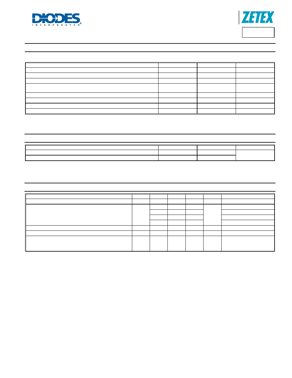
Maximum Ratings
@T
A
= 25°C unless otherwise specified
Single phase, half wave, 60Hz, resistive or inductive load.
For capacitance load, derate current by 20%.
Characteristic Symbol
Value
Unit
DC Blocking Voltage
V
RM
40 V
Continuous Forward current
I
F
380 mA
Average Peak Forward Current; duty cycle = 50%
I
FAV
650 mA
Non-Repetitive Forward Current
@ t < 100µs
@ t < 10ms
I
FSM
6.0
1.3
A
Power Dissipation at T
A
= +25°C (Note 5)
P
D
357 mW
Power Dissipation at T
A
= +25°C (Note 6)
P
D
413 mW
Operating and storage temperature range
T
STG
-55 to +150
°C
Junction Temperature
T
J
+150 °C
Thermal Characteristics
Characteristic Symbol
Value
Unit
Thermal Resistance Junction to Ambient (Note 5)
R
θJA
350
°C/W
Thermal Resistance Junction to Ambient (Note 6)
R
θJA
303
Electrical Characteristics
@T
A
= 25°C unless otherwise specified
Characteristic Symbol
Min
Typ
Max
Unit
Test
Condition
Reverse Breakdown Voltage
V
(BR)R
40 53 — V
I
R
= 100 µA
Forward Voltage Drop (Note 7)
V
F
—
395 450
mV
I
F
= 30mA
—
430 520
I
F
= 50mA
—
490 635
I
F
= 100mA
—
650 1000
I
F
= 275mA
Leakage Current
I
R
—
0.15 4 µA
V
R
= 30V
Total Capacitance
C
T
—
2.5 6 —
f = 1MHz; V
R
= 30V
Reverse Recovery Time
t
rr
— 1 — nS
Switch from I
F
= 100mA to
I
R
= 100mA.
Measured at I
R
= 10mA
Notes:
5. For a single device surface mounted on 25mm x 25mm x 1.6mm FR4 PCB with high coverage of 1oz copper in still air conditions
6. As above measured @ t < 5 seconds
7. Measured under pulsed conditions. Pulse width ≤ 300µs; duty cycle ≤ 2%