Diodes SBR2A40P1 User Manual
Sbr2a40p1, Features, Mechanical data
SBR2A40P1
Document number: DS30919 Rev. 10 - 2
1 of 5
April 2010
© Diodes Incorporated
SBR2A40P1
SBR and PowerDI are registered trademarks of Diodes Incorporated.
2.0A SBR
®
SURFACE MOUNT SUPER BARRIER RECTIFIER
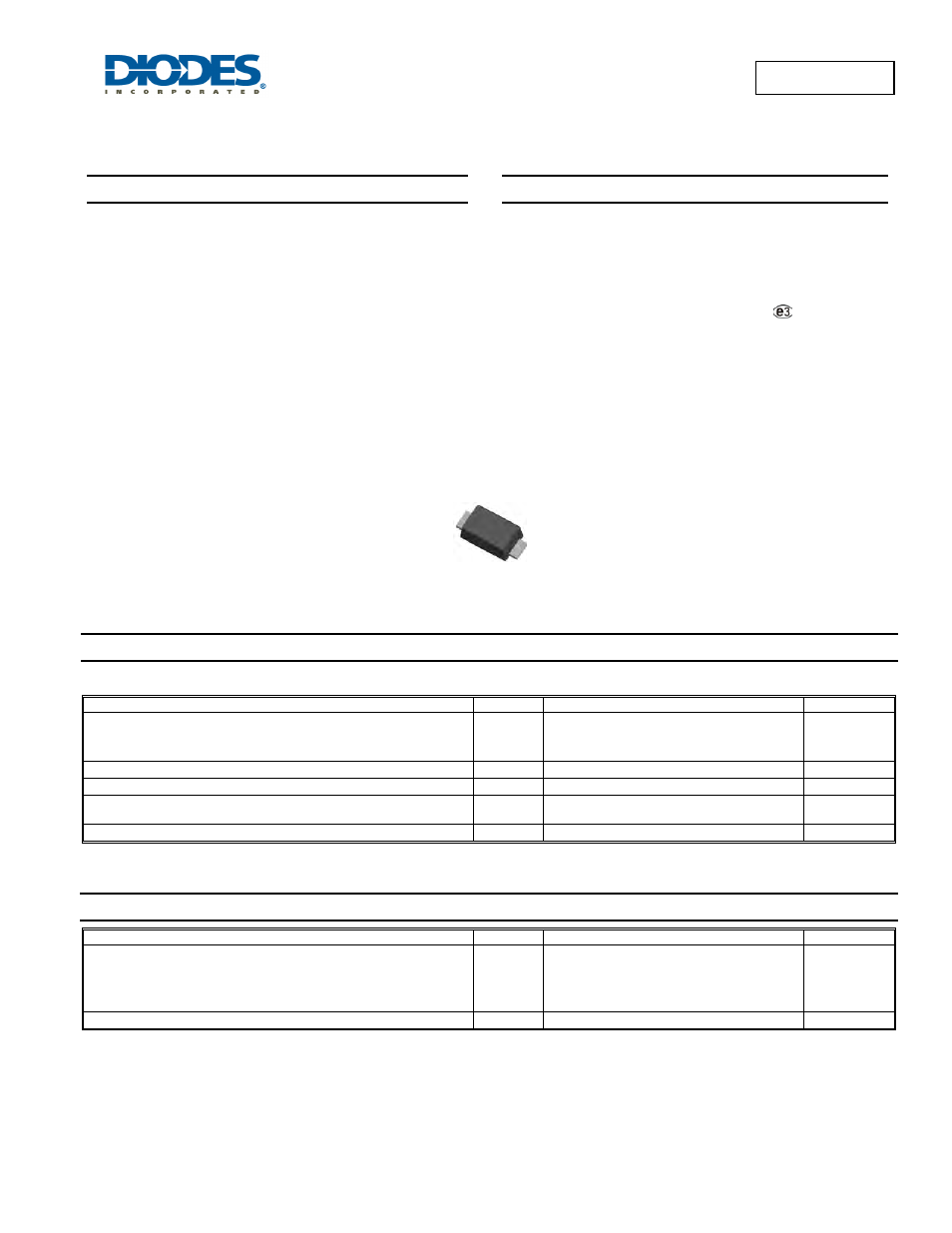
PowerDI
®
123
Features
•
Low Forward Voltage Drop
• Low
Leakage
Current
•
Superior Reverse Avalanche Capability
•
Excellent High Temperature Stability
•
Patented Interlocking Clip Design for High Surge Current
Capacity
•
Patented Super Barrier Rectifier Technology
•
Soft, Fast Switching Capability
•
150ºC Operating Junction Temperature
•
±16KV ESD Protection (HBM, 3B)
•
±25KV ESD Protection (IEC61000-4-2 Level 4, Air Discharge)
•
Lead Free Finish, RoHS Compliant (Note 1)
•
“Green” Molding Compound (No Br, Sb)
•
Qualified to AEC-Q 101 Standards for High Reliability
Mechanical Data
• Case:
PowerDI
®
123
•
Case Material: Molded Plastic, “Green” Molding Compound.
UL Flammability Classification Rating 94V-0
•
Moisture Sensitivity: Level 1 per J-STD-020
•
Polarity Indicator: Cathode Band
•
Terminals: Finish - Matte Tin annealed over Copper leadframe.
Solderable per MIL-STD-202, Method 208
•
Marking Information: See Page 4
•
Ordering Information: See Page 4
•
Weight: 0.018 grams (approximate)
Maximum Ratings
@T
A
= 25°C unless otherwise specified
Single phase, half wave, 60Hz, resistive or inductive load.
For capacitance load, derate current by 20%.
Characteristic Symbol
Value
Unit
Peak Repetitive Reverse Voltage
Working Peak Reverse Voltage
DC Blocking Voltage
V
RRM
V
RWM
V
RM
40 V
RMS Reverse Voltage
V
R(RMS)
28 V
Average Rectified Output Current (See Figure 1)
I
O
2.0 A
Non-Repetitive Peak Forward Surge Current 8.3ms
Single Half Sine-Wave Superimposed on Rated Load
I
FSM
50 A
Repetitive Peak Avalanche Power (1
μs, 25°C)
P
ARM
6,000 W
Thermal Characteristics
Characteristic Symbol
Value
Unit
Maximum Thermal Resistance
Thermal Resistance Junction to Soldering (Note 2)
Thermal Resistance Junction to Ambient (Note 3)
Thermal Resistance Junction to Ambient (Note 4)
R
θJS
R
θJA
R
θJA
5
180
115
ºC/W
Operating and Storage Temperature Range
T
J
, T
STG
-65 to +150
ºC
Notes:
1. EU Directive 2002/95/EC (RoHS). All applicable RoHS exemptions applied, see EU Directive 2002/95/EC Annex Notes.
2. Theoretical R
θJS
calculated from the top center of the die straight down to the PCB cathode tab solder junction.
3. FR-4 PCB, 2 oz. Copper, minimum recommended pad lay4. Polymide PCB, 2 oz. Copper, minimum recommended pad layout pe
Top View