Sbr1u30sv, Package outline dimensions, Suggested pad layout – Diodes SBR1U30SV User Manual
Page 3
SBR1U30SV
Document number: DS35028 Rev. 4 - 2
3 of 4
April 2013
© Diodes Incorporated
SBR1U30SV
SBR is a registered trademark of Diodes Incorporated.
V , DC REVERSE VOLTAGE (V)
R
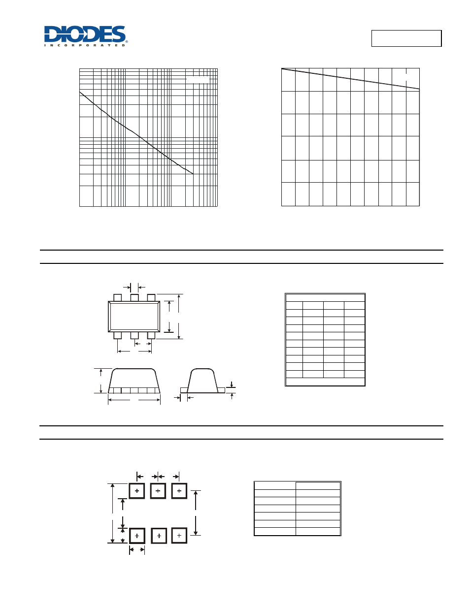
Figure 3 Total Capacitance vs. Reverse Voltage
C
, T
O
TAL
C
A
P
A
C
IT
A
N
C
E (
pF)
T
10
100
1000
0.1
1
10
100
f = 1MHz
0
3
6
9
12
15 18
21 24
27 30
V , DC REVERSE VOLTAGE (V)
R
Figure 4 Operating Temperature Derating
T
, DE
R
A
T
ED AM
BI
E
N
T
T
EM
P
E
R
A
T
U
R
E (
°C
)
A
0
25
50
75
100
125
150
Note 5
Package Outline Dimensions
rsion.
Suggested Pad Layout
e latest version.
SOT563
Dim
Min
Max Typ
A
0.15
0.30 0.20
B
1.10
1.25 1.20
C
1.55
1.70 1.60
D
-
-
0.50
G
0.90
1.10 1.00
H
1.50
1.70 1.60
K
0.55
0.60 0.60
L
0.10
0.30 0.20
M
0.10
0.18 0.11
All Dimensions in mm
Dimensions Value (in mm)
Z
2.2
G
1.2
X
0.375
Y
0.5
C1
1.7
C2
0.5
A
M
L
B
C
H
K
G
D
X
Z
Y
C1
C2
C2
G
- PDS3200 (5 pages)
- PDS340 (5 pages)
- PDS340Q (5 pages)
- PDS360 (5 pages)
- PDS360Q (5 pages)
- PDS4150 (4 pages)
- PDS3100Q (5 pages)
- PDS3100 (5 pages)
- PDS1240CTL (5 pages)
- PDS1045 (5 pages)
- PDS1040L (5 pages)
- PDS1040CTL (5 pages)
- PDS1040 (5 pages)
- PD3S230L (5 pages)
- PD3S230H (3 pages)
- PDS5100Q (5 pages)
- PDS835L (5 pages)
- PDS760 (5 pages)
- PDS560 (5 pages)
- PDS540 (5 pages)
- PDS5100H (5 pages)
- PDS5100 (5 pages)
- PDS4200H (6 pages)
- SBL3060CTP (4 pages)
- SBL30L30CT (3 pages)
- SBL3045CTP (4 pages)
- SBL3040CTP (4 pages)
- SBL2060CTP (4 pages)
- SBL2030CT - SBL2060CT (3 pages)
- SBL2045CTP (4 pages)
- SBL1060CTP (4 pages)
- SBL1040CTP (4 pages)
- SBG3030CT - SBG3045CT (5 pages)
- SB520 - SB560 (3 pages)
- SB370 - SB3100 (3 pages)
- SB320 - SB360 (3 pages)
- SBR10U100CT (5 pages)
- SBR10U150CT (5 pages)
- SBR10A45SP5 (5 pages)
- SBR1060CT (5 pages)
- SBR1045SP5 (5 pages)
- SBR1045SD1 (4 pages)
- SBR1045D1 (5 pages)
- SBR1045CTL (4 pages)
- SBR1040CT (5 pages)