Detailed description – Rainbow Electronics MAX1495 User Manual
Page 9

MAX1491/MAX1493/MAX1495
3.5- and 4.5-Digit, Single-Chip
ADCs with LCD Drivers
_______________________________________________________________________________________
9
Detailed Description
The MAX1491/MAX1493/MAX1495 low-power, highly
integrated ADCs with LCD drivers convert a ±2V differ-
ential input voltage (one count is equal to 100µV for the
MAX1493/MAX1495 and 1mV for the MAX1491) with a
sigma-delta ADC and output the result to an LCD. An
additional ±200mV input range (one count is equal to
10µV for the MAX1493/MAX1495 and 100µV for the
MAX1491) is available to measure small signals with
increased resolution.
These devices operate from a single 2.7V to 5.25V power
supply and offer 3.5-digit (MAX1491) or 4.5-digit
(MAX1493/MAX1495) conversion results. An internal
2.048V reference, internal charge pump and a high-accu-
racy on-chip oscillator eliminate external components.
These devices also feature on-chip buffers for the dif-
ferential input signal and external reference inputs,
allowing direct interface with high-impedance signal
sources. In addition, they use continuous internal offset
calibration, and offer >100dB of 50Hz and 60Hz line
noise rejection. Other features include data hold and
peak hold, and a low-battery monitor. The MAX1495
also performs enhanced offset calibration on demand.
Analog Input Protection
Internal protection diodes limit the analog input range
from V
NEG
to (AV
DD
+ 0.3V). If the analog input
exceeds this range, limit the input current to 10mA.
Internal Analog Input/
Reference Buffers
The MAX1491/MAX1493/MAX1495 analog input/refer-
ence buffers allow the use of high-impedance signal
sources. The input buffers’ common-mode input range
allows the analog inputs and reference to range from
-2.2V to +2.2V.
Modulator
The MAX1491/MAX1493/MAX1495 perform analog-to-
digital conversions using a single-bit, 3rd-order, sigma-
delta modulator. The sigma-delta modulation converts
the input signal into a digital pulse train whose average
duty cycle represents the digitized signal information.
The modulator quantizes the input signal at a much
higher sample rate than the bandwidth of the input.
The MAX1491/MAX1493/MAX1495 modulator provides
3rd-order frequency shaping of the quantization noise
resulting from the single-bit quantizer. The modulator is
fully differential for maximum signal-to-noise ratio and
minimum susceptibility to power-supply noise. A single-
bit data stream is then presented to the digital filter for
processing, to remove the frequency-shaped quantiza-
tion noise.
Digital Filtering
The MAX1491/MAX1493/MAX1495 contain an on-chip
digital lowpass filter that processes the data stream
from the modulator using a SINC4 (sinx/x)
4
response.
The SINC
4
filter has a settling time of four output data
periods (4 x 200ms).
The MAX1491/MAX1493/MAX1495 have 25% overrange
capability built into the modulator and digital filter:
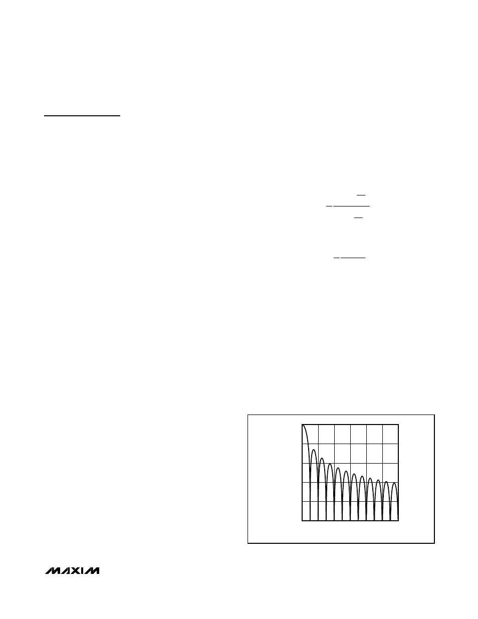
Filter Characteristics
Figure 2 shows the filter frequency response. The SINC
4
characteristic -3dB cutoff frequency is 0.228 times the
first notch frequency (5Hz). The oversampling ratio
(OSR) for the MAX1491 is 128 and the OSR for the
MAX1493/MAX1495 is 1024.
The output data rate for the digital filter corresponds
with the positioning of the first notch of the filter’s fre-
quency response. The notches of the SINC
4
filter are
repeated at multiples of the first notch frequency. The
SINC
4
filter provides an attenuation of better than
100dB at these notches. For example, 50Hz is equal to
10 times the first notch frequency and 60Hz is equal to
12 times the first notch frequency.
H z
N
z
z
( )
=
( )
( )
⎡
⎣
⎢
⎢
⎢
⎤
⎦
⎥
⎥
⎥
1
1
1
1
4
-
-
-N
-
H f
N
N
f
f
f
f
m
m
( )
sin
sin
=
⎛
⎝⎜
⎞
⎠⎟
⎛
⎝⎜
⎞
⎠⎟
⎡
⎣
⎢
⎢
⎢
⎢
⎢
⎤
⎦
⎥
⎥
⎥
⎥
⎥
1
4
π
π
FREQUENCY (Hz)
GAIN (dB)
50
40
30
20
10
-160
-120
-80
-40
0
-200
0
60
Figure 2. Frequency Response of the SINC
4
Filter (Notch at 60Hz)
