Applications information – Rainbow Electronics MAX1495 User Manual
Page 17
MAX1491/MAX1493/MAX1495
3.5- and 4.5-Digit, Single-Chip
ADCs with LCD Drivers
______________________________________________________________________________________
17
If ghosting is present on the LCD, the RMS OFF voltage
is too high. Choose an LCD with a higher RMS OFF
voltage or decrease DV
DD
.
Decimal Point Control
The MAX1491/MAX1493/MAX1495 allow for full deci-
mal-point control and feature leading-zero suppression.
Use DPON, DPSET1, and DPSET2 to set the value of
the decimal point. Tables 2 and 3 show the truth tables
of the DPON, DPSET1, and DPSET2 that determine
which decimal point is used.
Reference
The MAX1491/MAX1493/MAX1495 reference sets the
full-scale range of the ADC transfer function. With a
nominal 2.048V reference, the ADC full-scale range is
±2V with RANGE equal to GND. With RANGE equal to
DV
DD
, the full-scale range is ±200mV. A decreased ref-
erence voltage decreases full-scale range (see the
Transfer Functions section).
The MAX1491/MAX1493/MAX1495 accept either an
external reference or an internal reference. The INTREF
input selects the reference mode.
For internal reference operation, connect INTREF to
DV
DD
, connect REF- to GND, and bypass REF+ to
GND with a 4.7µF capacitor. The internal reference pro-
vides a nominal 2.048V source between REF+ and
GND. The internal reference temperature coefficient is
typically 40ppm/°C.
Connect INTREF to GND to use the external reference.
The external reference inputs, REF+ and REF-, are fully
differential. For a valid external reference input, V
REF+
must be greater than V
REF-
. Bypass REF+ and REF-
with a 0.1µF or greater capacitor to GND in external ref-
erence mode.
Figure 13 shows the MAX1493/MAX1495 operating with
an external differential reference. In this mode, REF- is
connected to the top of the strain gauge and REF+ is
connected to the midpoint of the resistor-divider on the
supply.
Applications Information
Power-On
At power-on, the digital filter and modulator circuits
reset. The MAX1493/MAX1495 allow 6s for the refer-
ence to stabilize before performing enhanced offset
calibration. During these 6s, the MAX1493/MAX1495
display 1.2V to 1.5V when a stable reference is detect-
ed. If a valid reference is not found, the MAX1493/
MAX1495 time out after 6s and begin enhanced offset
calibration. Enhanced offset calibration typically lasts
2s. The MAX1493/MAX1495 begin converting after
enhanced offset calibration.
Offset Calibration
The MAX1491/MAX1493/MAX1495 offer on-chip offset
calibration. The MAX1491/MAX1493/MAX1495 calibrate
offset during every conversion cycle. The MAX1495
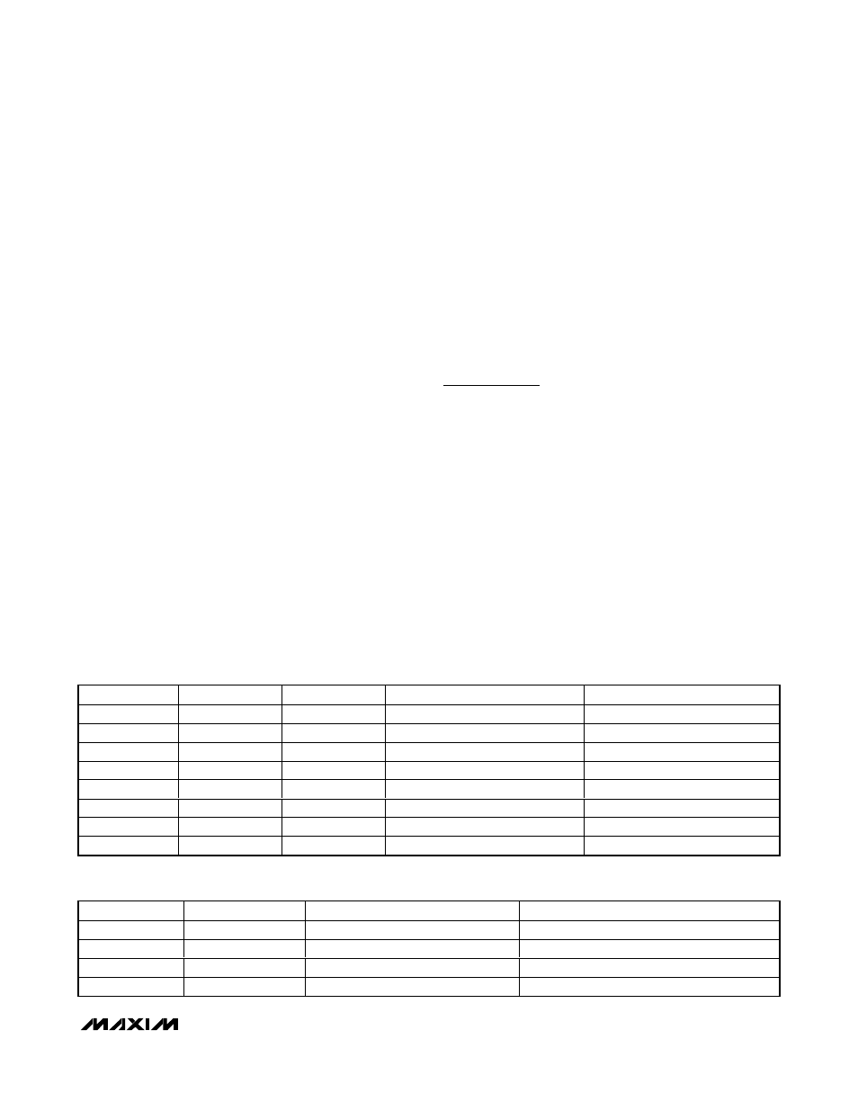
Table 2. Decimal-Point Control Table (MAX1493/MAX1495)
DPON
DPSET1
DPSET2
DISPLAY OUTPUT
ZERO INPUT READING
0
0
0
1 8 8 8 8
0
0
0
1
1 8 8 8 8
0
0
1
0
1 8 8 8 8
0
0
1
1
1 8 8 8 8
0
1
0
0
1 8 8 8.8
0.0
1
0
1
1 8 8.8 8
0.00
1
1
0
1 8.8 8 8
0.000
1
1
1
1.8 8 8 8
0.0000
Table 3. Decimal-Point Control Table (MAX1491)
DPSET1
DPSET2
DISPLAY OUTPUT
ZERO INPUT READING
0
0
1 8 8.8
0.0
0
1
1 8.8 8
0.00
1
0
1.8 8 8
0.000
1
1
1 8 8 8
000