Wide brightness range ccfl backlight controllers – Rainbow Electronics MAX1839 User Manual
Page 21
MAX1739/MAX1839
†
Wide Brightness Range
CCFL Backlight Controllers
______________________________________________________________________________________
21
has three identification (ID) registers: an 8-bit chip ID
register, an 8-bit chip revision register, and an 8-bit
manufacturer ID register.
The CRF/SDA and CTL/SCL pins have Schmidt-trig-
gered inputs that can accommodate slow edges; how-
ever, the rising and falling edges should still be faster
than 1µs and 300ns, respectively.
Communication starts with the master signaling the
beginning of a transmission with a START condition,
which is a high-to-low transition on CRF/SDA while
CTL/SCL is high. When the master has finished com-
municating with the slave, the master issues a STOP
condition (P), which is a low-to-high transition on
CRF/SDA while CTL/SCL is high (Figures 10, 11). The
bus is then free for another transmission. Figures 12
and 13 show the timing diagram for signals on the
2-wire interface. The address byte, command byte, and
data byte are transmitted between the START and
STOP conditions. The CRF/SDA state is allowed to
change only while CTL/SCL is low, except for the
START and STOP conditions. Data is transmitted in 8-
bit words and is sampled on the rising edge of
CTL/SCL. Nine clock cycles are required to transfer each
byte in or out of the MAX1739 since either the master or
the slave acknowledges the receipt of the correct byte
during the ninth clock. If the MAX1739 receives its correct
slave address followed by RW = 0, it expects to receive 1
or 2 bytes of information (depending on the protocol). If
the device detects a start or stop condition prior to clock-
ing in the bytes of data, it considers this an error condition
and disregards all of the data. If the transmission is com-
pleted correctly, the registers are updated immediately
after a STOP (or RESTART) condition. If the MAX1739
receives its correct slave address followed by RW = 1, it
expects to clock out the register data selected by the pre-
vious command byte.
SMBus Commands
The MAX1739 registers are accessible through several
different redundant commands (i.e., the command byte
in the read-byte and write-byte protocols), which can
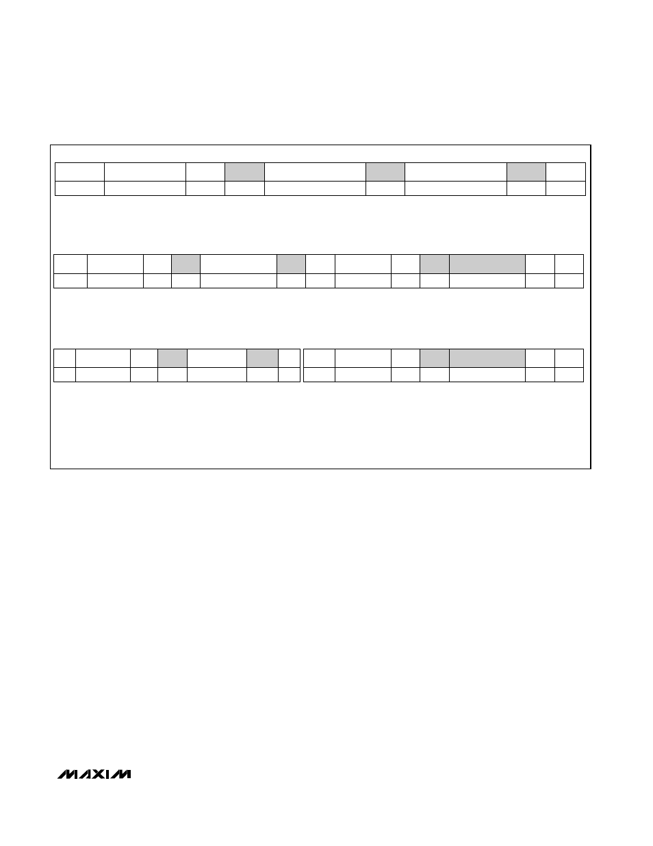
1b
ACK
1b
7 bits
ADDRESS
ACK
1b
WR
8 bits
DATA
1b
ACK
P
8 bits
S
COMMAND
Write-Byte Format
Receive-Byte Format
Slave Address
Command Byte: selects
which register you are
writing to
Data Byte: data goes into the register
set by the command byte
1b
ACK
1b
7 bits
ADDRESS
ACK
1b
WR
S
1b
ACK
8 bits
DATA
7 bits
ADDRESS
1b
RD
1b
8 bits
///
P
S
COMMAND
Slave Address
Slave Address
Command Byte: sends command
with no data; usually used for one-
shot command
Command Byte: selects
which register you are
reading from
Slave Address: repeated
due to change in data-
flow direction
Data Byte: reads from
the register set by the
command byte
1b
ACK
7 bits
ADDRESS
1b
RD
8 bits
DATA
1b
///
P
S
Data Byte: reads data from
the register commanded
by the last read-byte or
write-byte transmission;
also used for SMBus Alert
Response return address
S = Start condition
Shaded = Slave transmission
WR = Write = 0
P = Stop condition
Ack= Acknowledged = 0
RD = Read =1
/// = Not acknowledged = 1
Figure 11. SMBus Protocols
1b
ACK
7 bits
ADDRESS
1b
WR
8 bits
COMMAND
1b
ACK
P
S
Send-Byte Format
Read-Byte Format