Rainbow Electronics MAX1362 User Manual
Page 10
MAX1361/MAX1362
Power Supply
The MAX1361 (2.7V to 3.6V) and MAX1362 (4.5V to
5.5V) operate from a single supply and consume
670µA (typ) at sampling rates up to 94.4ksps and
436µA in monitor mode at 150ksps. The MAX1361 fea-
tures a 2.048V internal reference and the MAX1362 fea-
tures a 4.096V internal reference. All devices can be
configured for use with an external reference from 1V to
V
DD
. Bypass V
DD
to GND using a 0.1µF or greater
ceramic capacitor for best performance.
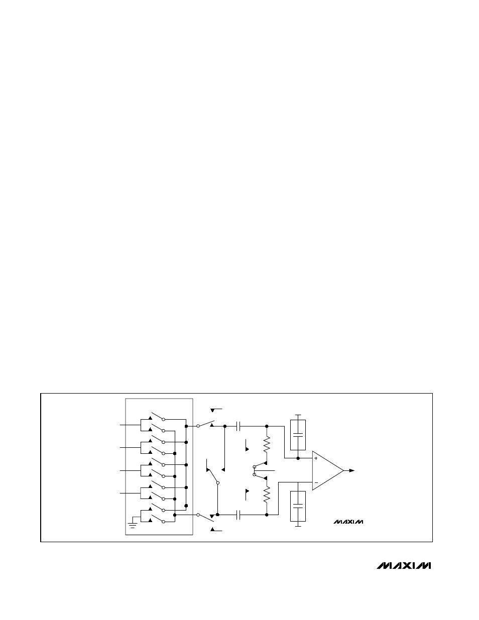
Analog Input and Track/Hold
The MAX1361/MAX1362 analog-input architecture con-
tains an analog-input multiplexer (MUX), fully differen-
tial T/H, comparator, and a fully differential switched
capacitive digital-to-analog converter (DAC). Figure 3
shows the equivalent input circuit for the MAX1361/
MAX1362.
In single-ended mode, the analog-input MUX connects
C
T/H
between the analog input selected by CS[3:0] and
GND (see the Configuration/Setup Bytes (Write Cycle)
section). In differential mode, the analog-input MUX
connects C
T/H
to the plus and minus analog inputs
selected by CS[3:0].
During the acquisition interval, the T/H switches are in
the track position, and C
T/H
charges to the analog-input
signal. At the end of the acquisition interval, the T/H
switches move to the hold position, retaining the
charge on C
T/H
as a stable sample of the input signal.
During the conversion, a switched capacitive DAC
adjusts to restore the comparator input voltage to 0V
within the limits of 10-bit resolution. This action requires
10 conversion clock cycles and is equivalent to trans-
ferring a charge of 11pF x (V
IN
+ - V
IN
-) from C
T/H
to the
binary-weighted capacitive DAC, forming a digital rep-
resentation of the analog-input signal.
Use a low source impedance to ensure an accurate
sample. A source impedance of up to 1.5k
Ω does not
significantly degrade sampling accuracy. For larger
source impedances, connect a 100pF capacitor from
the analog-input to GND or buffer the input.
In internal clock mode, the T/H circuitry enters track
mode on the eighth rising clock edge of the address
byte (see the Slave Address section). The T/H circuitry
enters hold mode on the falling clock edge of the
acknowledge bit of the address byte (the ninth clock
pulse). The conversions are then internally clocked, dur-
ing which time the MAX1361/MAX1362 hold SCL low.
In external clock mode, the T/H circuitry enters track
mode after a valid address on the rising edge of the
clock during the read bit (R/W = 1, bit 8). Hold mode is
entered on the rising edge of the second clock pulse
during the shifting out of the 1st byte of the result. The
next 10 clock cycles perform the conversions (see
Figure 13).
The time required for the T/H circuitry to acquire an
input signal is a function of the input sample capaci-
tance. If the analog-input source impedance is high,
the acquisition-time constant lengthens and more time
must be allowed between conversions. The acquisition
time (t
ACQ
) is the minimum time needed for the signal
to be acquired. It is calculated by:
t
ACQ
≥ 7 x (R
SOURCE
+ R
IN
) x C
IN
4-Channel, 10-Bit, System Monitor with Programmable
Trip Window and SMBus Alert Response
10
______________________________________________________________________________________
TRACK
TRACK
HOLD
C
T/H
C
T/H
TRACK
TRACK
HOLD
AIN0
AIN1
AIN2
AIN3/REF
ANALOG INPUT MUX
CAPACITIVE
DAC
REF
CAPACITIVE
DAC
REF
MAX1361
MAX1362
HOLD
HOLD
TRACK
HOLD
V
DD
/2
Figure 3. Equivalent Input Circuit