Max847 1-cell, step-up two-way pager system ic, Detailed description, Voltage regulators – Rainbow Electronics MAX847 User Manual
Page 9: Main dc-dc boost converter (out)

______________ Detailed Description
The MAX847 contains several functional blocks that
simplify the integration of power-supply and monitoring
functions within a 1-cell powered system. They are
described in the following subsections.
Voltage Regulators
Regulator outputs include the following:
• OUT: Main switch-mode boost output
• REG1: 1.5
Ω
switch and output voltage clamp. Switches
REG1 to OUT and clamps REG1 at 3.3V when OUT
is set to 3.4V or more.
• REG2: Linear-regulated, 24mA low-noise output that
regulates so that V
OUT
- V
REG2
is a set difference
voltage (10µA
•
R
OFS
). Output peak-to-peak ripple is
typically 2mV with a 10µF bypass capacitor at REG2.
REG2 clamps output at 3.3V.
• REG3: Low-noise, 1V linear regulator that supplies
2mA.
Main DC-DC Boost Converter (OUT)
OUT is the main DC-DC converter’s output. It supplies
current from the internal synchronous-rectified boost reg-
ulator and needs no external FETs or voltage-setting
resistors. The output voltage (V
OUT
) is adjusted from
1.8V to 4.9V in 100mV steps (Tables 2 and 6) by internal
DAC control using a serial-data command. OUT can
supply up to 80mA, less the current supplied to the other
regulators (REG1, REG2, and REG3).
OUT can also be put into a low-current, pulse-skipping
Coast Mode (13µA typical quiescent current) by reset-
ting the RUN/COAST serial input bit and holding the
RUN pin at 0V. OUT supplies up to 40mA in Coast
Mode. Typically, when changing from Run to Coast
Mode, a lower OUT voltage is also set (Table 5) to fur-
ther reduce system operating current. The extent of this
reduction depends on the minimum operating voltage
of the system components when they are in standby or
sleep states.
MAX847
1-Cell, Step-Up
Two-Way Pager System IC
_______________________________________________________________________________________
9
MAX847
AA ALKALINE
BATT
26
1
11
6
9
27
5
2
3
25
4
24
22
14
21
20
10
7
23
15
3.0V LOGIC
R6
2.85V ANALOG
TO RF PA
3-CELL
NiCd
R
OFS
15k
1V
RCVR
OUT
PGND
REG1
R2IN
OFS
REG2
L1
22
µ
H
MBRO52OL
C1
47
µ
F
C6
0.1
µ
F
CERAMIC
C2
10
µ
F
C3
10
µ
F
C4
1
µ
F
TO
µ
C RESET
R3
1.3M
R6
R4
470k
C7
C
OFS
0.1
µ
F
C10
1nF
C9
22nF
R7
10k
Ω
C8
0.1
µ
F
C5
22
µ
F
SERIAL
I/O
A/D IN
17
19
18
16
13
12
8
28
1.8
Ω
DRIVERS
38.4kHz
REG3
RSIN
RSO
NICD
AGND
RUN
LBI
R1
330k
R2
470k
R5
REG1
LBO
CH0
CS
SCL
SDI
SDO
DR1
DR2
DR2IN
DRGND
SYNC
FILT
REF
RUN
COAST
LX1
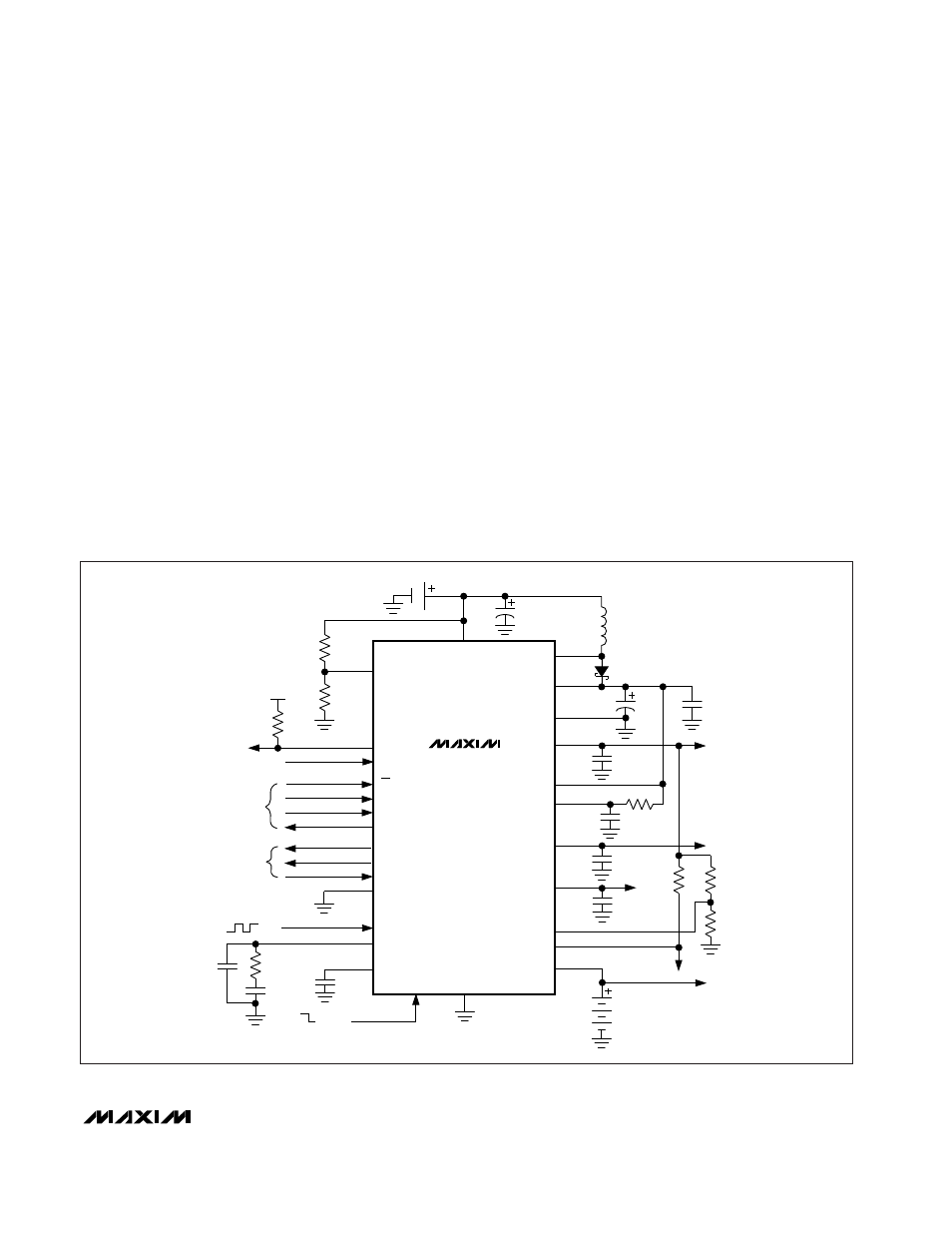
Figure 2. Standard Application Circuit
