Max847, Cell, step-up two-way pager system ic – Rainbow Electronics MAX847 User Manual
Page 10

MAX847
OUT can be set as low as 1.8V; however, some run
mode functions are limited when V
OUT
is below 2.5V:
• The allowed serial-interface clock rate is reduced.
• Internal LX FET and DR1 and DR2 on-resistance
increases.
Logic Supply (REG1)
REG1 is not a regulator in the conventional sense, but
rather a 1.5
Ω
PFET that acts as either a switch or a volt-
age clamp, depending on the programmed OUT volt-
age. When OUT is set to 3.3V or less, REG1 operates
as a switch. When OUT is set to 3.4V or more, the
REG1 output clamps at 3.3V. This arrangement limits
V
REG1
to an acceptable voltage for logic when OUT is
programmed to a higher voltage (typically >4V) for
charging (see
Charger Circuit
and
Backup Linear
Regulator
sections).
Low-Noise Analog Supply (REG2)
REG2 is a linear, 24mA low-dropout regulating circuit
whose input is R2IN. The REG2 output (V
REG2
) is set by
R
OFS
. R
OFS
does not set an absolute voltage, but rather
an offset level from R2IN (Figure 2). V
REG2
is set by:
V
REG2
= V
R2IN
- 10µA
·
R
OFS
Typically R2IN and R
OFS
are tied to OUT, in which
case:
V
OUT
- V
REG2
= 10µA
·
R
OFS
R
OFS
adjusts V
OUT
- V
REG2
to allow REG2 noise rejec-
tion to be traded for voltage drop and consequent effi-
ciency loss. A 15k
Ω
(typical) R
OFS
value sets a 150mV
voltage difference. R2IN typically is supplied from OUT
or REG1 but can be connected elsewhere as long as the
voltage applied to R2IN does not exceed V
OUT
. For low-
est output noise on REG2, connect R2IN to REG1.
Note that the REG2 output also clamps at 3.3V.
Low-Noise, 1V Analog Supply (REG3)
REG3 is a 1V, low-noise linear regulator that supplies up
to 2mA. REG3’s input is internally connected to REG2.
PWM Frequency Synchronization
The MAX847 DC-DC converter operates with or without
a clock at the SYNC input. If a SYNC clock is used, a
PLL filter network must be connected at FILT (see R7,
C9, and C10 in Figure 2). The DC-DC converter (in
Run Mode) operates at 7f
SYNC
. The MAX847 is
designed for a 38.4kHz SYNC clock and hence a
268.8kHz switching frequency. If a SYNC clock is not
used then FILT must be tied to REF and R7, C9, and
C10 should be omitted. Note that if a SYNC clock is not
used, and FILT is
not
connected to REF, the MAX847
will not enter Run Mode.
With no SYNC clock, and FILT tied to REF, the DC-DC
converter nominally operates at 270kHz when in Run
Mode. The Run Mode switching frequency has no rela-
tion to the serial-data clock rate.
On initial power-up, the MAX847 is designed to start in
Coast Mode, with Run Mode normally commanded by
system via the serial interface, or the RUN pin, after the
system has started. Under some circumstances, the
MAX847 may power up in Run Mode. These circum-
stances are:
1) If a SYNC clock is not used (REF tied to FILT).
2) If the SYNC clock is used and is provided at initial
power-up when REG1 is 1.5V or higher.
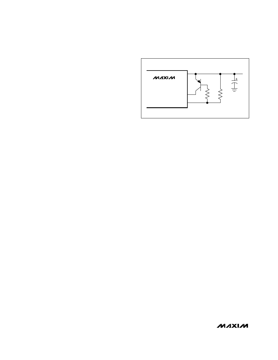
3) If the SYNC clock is used, the connection shown in
Figure 3 is added, and the SYNC clock is present
when RSO is cleared (logic high).
These choices are outlined in Table 1.
Voltage Detectors (LBO and Reset)
The MAX847 contains two voltage-detector inputs: LBI
and RSIN. The LBI and RSIN comparator outputs are
open-drain pins (LBO and RSO) for a real-time hard-
ware output. LBO is also readable via the serial inter-
face. Both LBI and RSIN trigger at a 0.6V input
threshold and have about 18mV hysteresis. RSO also
triggers the MAX847 internal power-on reset (POR).
7-Bit ADC (CH0 Input and CH1, CH2)
Three analog channels are compared to a 7-bit, serially
programmed digital-to-analog converter (CH DAC). The
CH DAC voltage can be varied in 10mV steps from
200mV to V
REF
- 1LSB (or 1.27V) (Table 2). CH0 is an
external input, while CH1 and CH2 are signals internally
generated from the NICD and BATT pins. NICD is inter-
nally divided by four before being compared to CH
DAC, while BATT directly connects to CH2.
1-Cell, Step-Up
Two-Way Pager System IC
10
______________________________________________________________________________________
MAX847
2N2907
Q1
OUT
FILT
RSO
25
12
7
C1
R8
1M
R6
1M
Figure 3. Add PNP to allow start-up in Run Mode before the
SYNC input clock is active.
