Max847 1-cell, step-up two-way pager system ic, Table 4. input-bit function description – Rainbow Electronics MAX847 User Manual
Page 13
Backup Linear Regulator
The BACKUP serial input bit turns on the backup regu-
lator, which sources current from NICD to OUT. This
regulator backs up OUT by using the rechargeable bat-
tery (at NICD) when the main battery (at BATT) is
depleted or removed. The backup regulator pass
device’s resistance is typically 5
Ω
, so it can typically
supply 20mA with only 100mV of dropout.
All DC-DC converter and charging circuitry is disabled
when the backup regulator is turned on, but all other
functions remain active. Activate BACKUP manually by
serial command, or set it to trigger automatically when
LBO goes low.
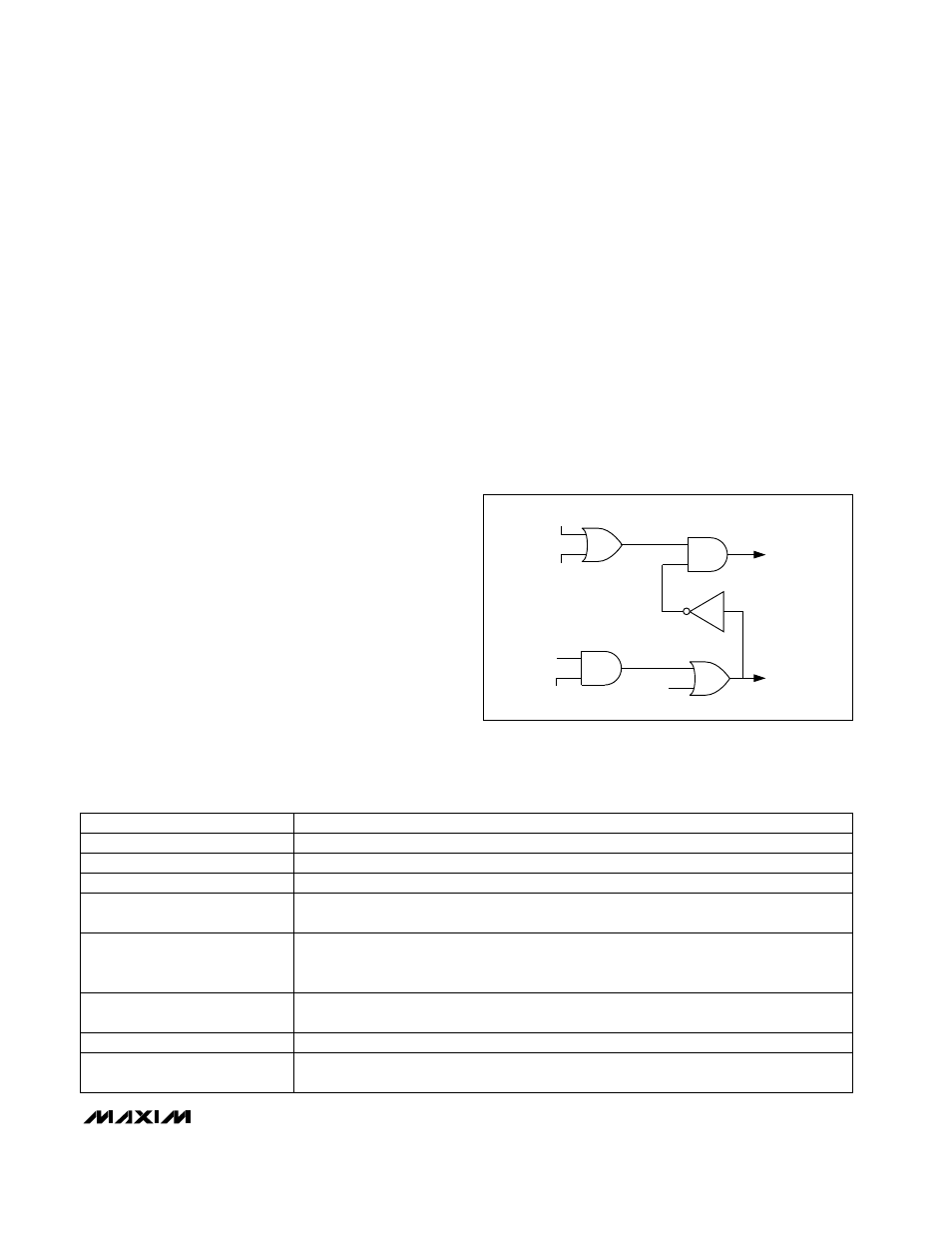
Automatic Backup
Setting the LBO_Sets_BACKUP serial bit (Table 2) pro-
grams the IC so that when LBO goes low, the backup
regulator automatically turns on without instructions
from the microprocessor (µP). When the LBO_
Sets_BACKUP bit is 0, the backup regulator is turned
on only by setting the BACKUP bit. The BACKUP bit
also overrides the LBO_Sets_BACKUP bit. Figure 4
shows the logic for this function.
If the main battery is depleted, and the NICD battery is
drained during backup, RSO goes low while the back-
up regulator is supplying OUT (if RSI is used to monitor
OUT or REG1). When RSO falls, the serial registers
reset to their POR states (with the DC-DC converter on
in Coast Mode and the backup regulator off, Tables 2,
3, and 4). This prevents the IC from getting hung up
with the DC-DC converter off when a new main battery
is inserted. This sequence is required because if the
MAX847 did not default to “DC-DC converter on” when
coming out of reset, the µP (still reset by RSO) would
not be able to provide the device with serial instructions
to turn on.
Serial Interface
The MAX847 has an SPI-compatible serial interface.
The serial-interface lines are Chip Select (CS), Serial
Clock (SCL), Serial Data In (SDI), and Serial Data Out
(SDO). Serial input data is arranged in 8-bit bytes. Most
bytes contain a 3-bit address pointer (R2, R1, R0)
along with 5 bits of input data (D4–D0). For common
operations such as selecting Run or Coast Mode, acti-
vating REG2 or REG3, or turning on DR1 or DR2, only
the 000 (R2, R1, R0) address register needs to be writ-
ten. The serial input data format for all MAX847 opera-
tions is outlined in Tables 2, 3, and 4.
MAX847
1-Cell, Step-Up
Two-Way Pager System IC
______________________________________________________________________________________
13
15mA_CHG
1mA_CHG
TO
CHARGER
CONTROL
TO
BACKUP
REGULATOR
BACKUP
LBO_SETS_BACKUP
LBO
Figure 4. Logic for Charger Control and BACKUP, and for
LBO_Sets_BACKUP Serial Input Bits
INPUT BIT
LBO_Sets_BACKUP
1 = Allow LBO to turn on backup regulator and disable DC-DC converter (POR state is no con-
nection between LBO and BACKUP).
OV0–OV4
RUN/COAST
Sets OUT Output Voltage (POR state is V
OUT
= 3.0V).
DAC0–DAC6
Sets 7-bit CH DAC voltage for A/D conversion (POR state is all zeros with DAC and compara-
tors off).
REG2_ON, REG3_ON
DR1, DR2
1mA_CHG, 15mA_CHG
FUNCTION
1 = Run Mode, 0 = Coast Mode (POR state is Coast Mode).
1 = Turn on selected regulator (POR state is off).
1 = Turn on selected switch (POR state is off).
1 = Turn on selected charge current to NICD. If both are set, the charge current is 15mA (POR
state is off).
BACKUP
1 = Turn on backup linear regulator from NICD to OUT and disable DC-DC converter (POR
state is BACKUP off). Setting this bit overrides 1mA_CHG, 15mA_CHG, and LBO_Sets_BACK-
UP (Figure 1).
Table 4. Input-Bit Function Description