Max847, Cell, step-up two-way pager system ic, Table 2. serial-bit assignments – Rainbow Electronics MAX847 User Manual
Page 12: Table 3. serial-bit power-on-reset (por) states
MAX847
pulse width modulation (PWM), as well as synchroniza-
tion, to minimize noise.
Some MAX847 functions are confined to Run Mode
while others remain active in both Run and Coast.
These are outlined as follows.
Various circuit functions can be disabled as follows:
Functions that
always remain on are:
• Serial I/O
• Reference (REF)
• OUT
• REG1
• LBI, RSIN (and LBO, RSO)
Functions that can be
programmed on or off
are (Table 1):
• DR1 and DR2
• REG2 and REG3
• NICD charger (Note: This may overload OUT if
turned on in Coast Mode when other loads are
present)
• NICD backup regulator
• CH0, CH1, CH2 and CH DAC
Functions that
always turn off in Coast Mode
are:
• SYNC and PLL circuits
• DC-DC PWM control circuits
Power-On Reset
The MAX847 has an internal POR circuit (V
OUT
< 1.6V)
to ensure an orderly power-up when a battery is first
applied. This feature is separate from the RSO com-
parator; however, if RSO goes low during operation, all
serial registers are set to the same predetermined
states as on power-up. The POR states for each regis-
ter are listed in Table 3.
Note that the MAX847 always comes out of reset in
Coast Mode; consequently, it cannot supply full power
until Run Mode is selected by either the RUN pin or ser-
ial command. System software cannot exercise full load
current until Run Mode is enabled.
Charger Circuit
A charger current source from OUT to NICD is activat-
ed via a serial bit (Table 2). The current source can
charge a small 3-cell NICD or NIMH battery (typically
coin cell) or a 1-cell lithium battery. The charge current
can be set to either 15mA or 1mA. When both 15mA
and 1mA are set, the charger runs at 15mA. OUT sets
the maximum charge (or float) voltage. When charging
is implemented, V
OUT
must also be set high enough to
allow sufficient headroom for the charger current
source. The V
OUT
- V
NICD
difference should normally
be between 0.2V and 0.5V. Charger current vs. output
voltage is graphed in the
Typical Operating
Characteristics
. Note also that charging current
reduces the OUT current available for other loads.
1-Cell, Step-Up
Two-Way Pager System IC
12
______________________________________________________________________________________
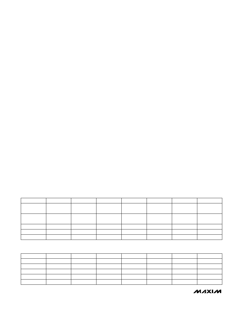
R2 (MSB)
R0
D3
D1
0
0
DR1_ON
REG2_ON
0
1
LBO_Sets_
BACKUP
15mA_CHG
0
0
OV3
OV1
0
1
X
X
Table 2. Serial-Bit Assignments
R1
0
0
1
1
D4
DR2_ON
X
OV4
X
D2
D0
RUN/
COAST
1mA_CHG
OV0
X
REG3_ON
BACKUP
OV2
X
1
DAC5
DAC3
DAC1
DAC6
DAC4
DAC0
DAC2
Table 3. Serial-Bit Power-On-Reset (POR) States
R2
R0
D3
D1
0
0
POR = 0
POR = 0
0
1
POR = 0
POR = 0
0
0
POR = 1
POR = 0
0
1
X
X
R1
0
0
1
1
D4
POR = 0
X
POR = 0
X
D2
D0
POR = 0
POR = 0
POR = 0
X
POR = 0
POR = 0
POR = 1
X
1
POR = 0
POR = 0
POR = 0
POR = 0
POR = 0
POR = 0
POR = 0