Max847 1-cell, step-up two-way pager system ic – Rainbow Electronics MAX847 User Manual
Page 2
MAX847
1-Cell, Step-Up
Two-Way Pager System IC
2
_______________________________________________________________________________________
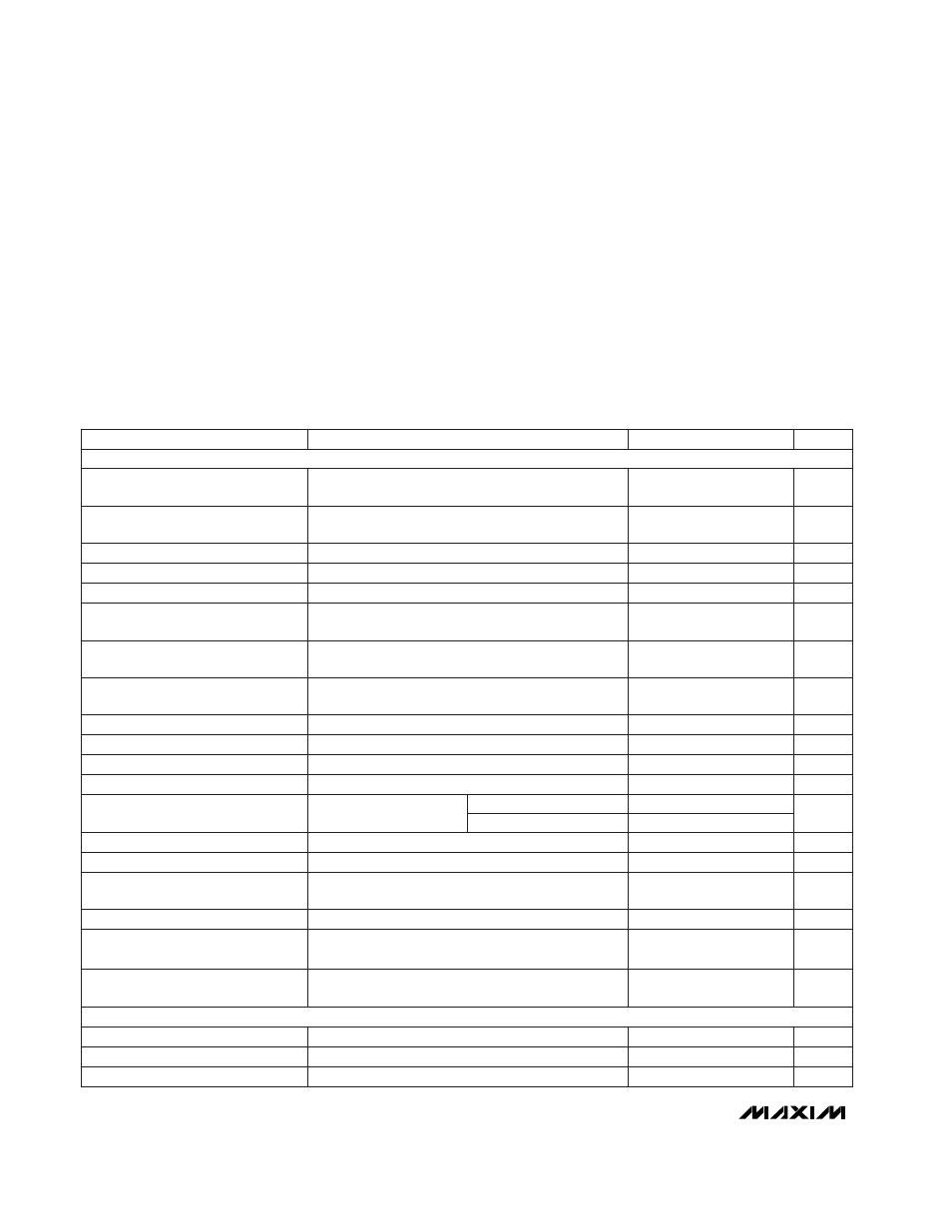
ABSOLUTE MAXIMUM RATINGS
ELECTRICAL CHARACTERISTICS
(OUT = 3.0V, BATT = 1.2V, NICD = 3.6V, T
A
= -40°C to +85°C, unless otherwise noted. Typical values are at T
A
= +25°C.) (Note 1)
Stresses beyond those listed under “Absolute Maximum Ratings” may cause permanent damage to the device. These are stress ratings only, and functional
operation of the device at these or any other conditions beyond those indicated in the operational sections of the specifications is not implied. Exposure to
absolute maximum rating conditions for extended periods may affect device reliability.
BATT, OUT, NICD, LBO, RSO to AGND...................-0.3V to +6V
REG1, OFS, REG2, REF, R2IN to AGND ...-0.3V to (OUT + 0.3V)
SCL, SDO, SDI,
CS , SYNC, FILT, DR2IN,
CH0, LBI, RSIN, RUN to AGND ...................-0.3V to (REG1 + 0.3V)
REG3 .......................................................-0.3V to (REG2 + 0.3V)
DR1, DR2 to DRGND ...............................-0.3V to (BATT + 0.3V)
PGND, DRGND to AGND ......................................-0.3V to +0.3V
LX1 to PGND .............................................-0.3V to (OUT + 0.3V)
Continuous Power Dissipation (T
A
= +70°C)
28-Pin QSOP (derate 8mW/°C above +70°C) .............640mW
Operating Temperature Range ...........................-40°C to +85°C
Junction Temperature ......................................................+150°C
Storage Temperature Range .............................-65°C to +165°C
Lead Temperature (soldering, 10sec) .............................+300°C
T
A
= +25°C
Run or Coast Mode
Incremental supply current when on
REG2, REG3 and CH DAC off, V
OUT
= 2.8V
REG2, REG3 and CH DAC on
Coast mode
Incremental supply current when on
CONDITIONS
V
0.9
1.1
BATT Minimum Start-Up Voltage
(Note 3)
V
0.8
OUT x
0.8
BATT Typical Operating Range
(Note 2)
µA
30
CH DAC Supply Current (Note 4)
µA
13
25
Coast Mode Supply Current (Note 4)
µA
875
1350
Run Mode Supply Current (Note 4)
µA
0.5
2
BATT Supply Current (Note 5)
µA
20
REG3 Supply Current (Note 4)
UNITS
MIN
TYP
MAX
PARAMETER
I
REF
= 0 to 20µA, OUT = 1.8V to 4.9V
V
-1.5%
1.28
1.5%
Reference Voltage
I
DR
= 120mA
Ω
1.8
2.8
DR1, DR2 On-Resistance
V
DR
= 5V
nA
1
250
DR1, DR2 Leakage Current
T
A
= +25°C
T
A
= -40°C to +85°C
I
SDO
= 100µA
mV
200
SDO Output Low
I
SDO
= -100µA, from REG1
V
V
REG1
- 0.2
SDO Output High
Includes CS, SDI, SCL, DR2IN, SYNC, and RUN
V
0.4
Logic Input Level Low
Includes CS, SDI, SCL, DR2IN, SYNC, and RUN
V
V
REG1
- 0.4
Logic Input Level High
3.6
50% duty cycle
MHz
5
SCL Maximum Clock Rate
ns
100
SDI Setup Time, t
DS
ns
50
SDI Hold Time, t
DH
Logic Input = 0 to 3.3V; includes CS, SDI, SCL,
DR2IN, SYNC, and RUN
µA
-1
1
Logic Input Current
Charger and Backup Modes off, NICD = 3.6V
µA
1.2
3
NICD Input Current, Standby
(Note 6)
Incremental supply current when on
µA
Backup mode, NICD = 3.6V, OUT = 3V
50
REG2 Supply Current (Note 4)
µA
20
40
NICD Input Supply Current, Backup
(Note 7)
Charger and Backup Modes off,
BATT = 0V and OUT = 0V
µA
1.2
3
NICD Input Current, Power Fail
(Note 8)
GENERAL PERFORMANCE
SERIAL-INTERFACE TIMING SPECIFICATIONS
(Note 9)