Max1422, Detailed description, Pin description – Rainbow Electronics MAX1422 User Manual
Page 8
MAX1422
Detailed Description
The MAX1422 uses a 12-stage, fully-differential,
pipelined architecture (Figure 1), that allows for high-
speed conversion while minimizing power consump-
tion. Each sample moves through a pipeline stage
every half-clock cycle. Including the delay through the
output latch, the latency is seven clock cycles.
A 2-bit (2-comparator) flash ADC converts the held-
input voltage into a digital code. The following digital-
to-analog converter (DAC) converts the digitized result
back into an analog voltage, which is then subtracted
from the original held-input signal. The resulting error
signal is then multiplied by two and the product is
passed along to the next pipeline stage. This process
is repeated until the signal has been processed by all
12 stages. Each stage provides a 1-bit resolution.
Digital error correction compensates for ADC compara-
tor offsets in each pipeline stage and ensures no
missing codes.
12-Bit, 20Msps, +3.3V, Low-Power ADC with
Internal Reference
8
_______________________________________________________________________________________
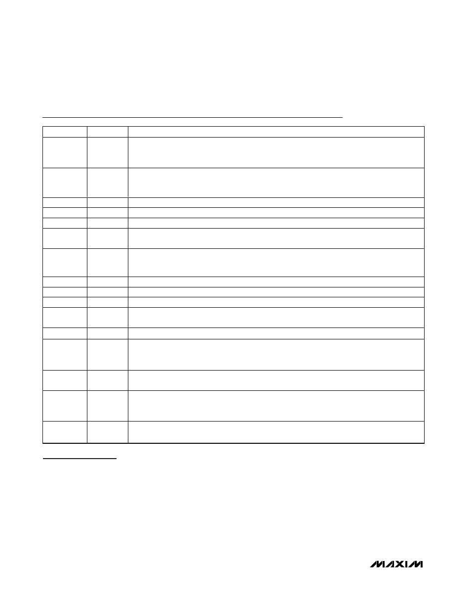
Pin Description
PIN
NAME
FUNCTION
1, 4, 5, 8, 9,
12, 13, 16,
19, 41, 48
AGND
Analog Ground. Connect all return paths for analog signals to AGND.
2, 3, 10, 11,
14, 15, 20,
42, 47
AV
DD
Analog Supply Voltage. For optimum performance, bypass to the closest AGND with a parallel
combination of a 0.1
µF, and a 1nF capacitor. Connect a single 10µF and 1µF capacitor combination
between AV
DD
and AGND.
6
INP
Positive Analog Signal Input
7
INN
Negative Analog Signal Input
17
CLK
Clock Frequency Input. Clock frequency input ranges from 100kHz to 20MHz.
18
CLK
Complementary Clock Frequency Input. This input is used for differential clock input. If the ADC is
driven with a single-ended clock, bypass
CLK with 0.1
µF capacitor to AGND.
21, 31, 32
DV
DD
Digital Supply Voltage. For optimum performance, bypass to the closest DGND with a parallel
combination of a 0.1
µF and a 1nF capacitor. Connect a single 10µF and 1µF capacitor combination
between DV
DD
and DGND.
22, 29, 30
DGND
Digital Ground
23–28
D0–D5
Digital Data Outputs. Data bits D0 through D5, where D0 represents the LSB.
33–38
D6–D11
Digital Data Outputs. D6 through D11, where D11 represents the MSB.
39
OE
Output Enable Input. A logic "1" on
OE places the outputs D0–D11 into a high-impedance state. A
logic "0" allows for the data bits to be read from the outputs.
40
PD
Shutdown Input. A logic "1" on PD places the ADC into shutdown mode.
43
REFIN
External Reference Input. Bypass to AGND with a capacitor combination of 0.22
µF in parallel with
1nF. REFIN can be biased externally to adjust reference levels and calibrate full-scale errors. To
disable the internal reference, connect REFIN to AGND.
44
REFP
Positive Reference I/O. Bypass to AGND with a capacitor combination of 0.22
µF in parallel with 1nF.
With the internal reference disabled (REFIN = AGND), REFP should be biased toV
CML
+ V
DIFF
/2.
45
REFN
Negative Reference I/O. Bypass to AGND with a capacitor combination of 0.22
µF in parallel with
1nF. With the internal reference disabled (REFIN = AGND), REFN should be biased to
V
CML
- V
DIFF
/2.
46
CML
Common-Mode Level Input. Bypass to AGND with a capacitor combination of 0.22
µF in parallel with
1nF. With the internal reference disabled (REFIN = AGND).