Rainbow Electronics MAX1422 User Manual
Page 2
MAX1422
12-Bit, 20Msps, +3.3V, Low-Power ADC with
Internal Reference
2
_______________________________________________________________________________________
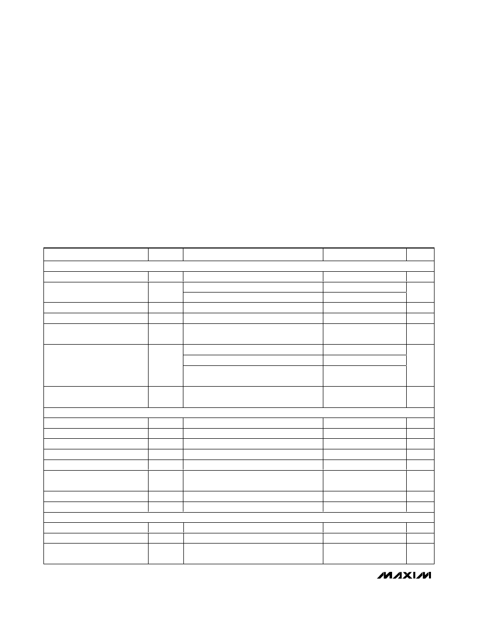
ABSOLUTE MAXIMUM RATINGS
ELECTRICAL CHARACTERISTICS
(V
AVDD
= V
DVDD
= +3.3V, AGND = DGND = 0, V
IN
= ±1.024V, differential input voltage at -0.5dB FS, internal reference, f
CLK
= 20MHz
(50% duty cycle), digital output load C
L
≈ 10pF, T
A
= T
MIN
to T
MAX
, unless otherwise noted. Typical values are at T
A
= +25°C.)
Stresses beyond those listed under “Absolute Maximum Ratings” may cause permanent damage to the device. These are stress ratings only, and functional
operation of the device at these or any other conditions beyond those indicated in the operational sections of the specifications is not implied. Exposure to
absolute maximum rating conditions for extended periods may affect device reliability.
AV
DD
, DV
DD
to AGND ..............................................-0.3V to +4V
DV
DD
, AV
DD
to DGND..............................................-0.3V to +4V
DGND to AGND.....................................................-0.3V to +0.3V
INP, INN, REFP, REFN, REFIN,
CML,CLK, CLK, ....................(AGND - 0.3V) to (AV
DD
+ 0.3V)
D0–D11, OE, PD .......................(DGND - 0.3V) to (DV
DD
+ 0.3V)
Continuous Power Dissipation (T
A
= +70°C)
48-Pin TQFP (derate 12.5mW/°C above +70°C)........1000mW
Operating Temperature Ranges
MAX1422CCM ....................................................0°C to +70°C
MAX1422ECM .................................................-40°C to +85°C
Maximum Junction Temperature .....................................+150°C
Storage Temperature Range .............................-65°C to +150°C
Lead Temperature (soldering, 10s) .................................+300°C
PARAMETER
SYMBOL
CONDITIONS
MIN
TYP
MAX
UNITS
DC ACCURACY
Resolution
RES
12
bits
T
A
= +25
°C, no missing codes
-1
1
Differential Nonlinearity
DNL
T
A
= T
MIN
to T
MAX
±0.5
LSB
Integral Nonlinearity
INL
T
A
= T
MIN
to T
MAX
±2
LSB
Mid-scale Offset
MSO
-3
±.75
3
%FSR
Mid-scale Offset Temperature
Coefficient
MSOTC
3
✕
10
- 4
%/
°C
Internal reference (Note 1)
-5
±0.1
5
External reference applied to REFIN, (Note 2)
-5
±0.2
5
Gain Error
GE
External reference applied to REFP, CML,
and REFN (Note 3)
-1.5
1.5
%FSR
Gain Error Temperature
Coefficient
GETC
External reference applied to REFP, CML,
and REFN (Note 3)
15
✕
10
- 6
%/
°C
DYNAMIC PERFORMANCE (f
CLK
= 20MHz, 4096-point FFT)
Signal-to-Noise Ratio
SNR
f
IN
= 5MHz, T
A
= +25
°C
63
67
dB
Spurious-Free Dynamic Range
SFDR
f
IN
= 5MHz, T
A
= +25
°C
64
74
dBc
Total Harmonic Distortion
THD
f
IN
= 5MHz, T
A
= +25
°C
-72
-63
dBc
Signal-to-Noise and Distortion
SINAD
f
IN
= 5MHz, T
A
= +25
°C
60
65
dB
Effective Number of Bits
ENOB
f
IN
= 5MHz
10.5
Bits
Two-Tone Intermodulation
Distortion
IMD
f
IN1
= 7.028MHz, f
IN2
= 8.093MHz (Note 4)
-77
dBc
Differential Gain
DG
±1
%
Differential Phase
DP
±0.25
degrees
ANALOG INPUTS (INP, INN, CML)
Input Resistance
R
IN
Either input to ground
61
k
Ω
Input Capacitance
C
IN
Either input to ground
4
pF
Common-Mode Input Level
(Note 5)
V
CML
V
AV DD
✕
0.5
V