Applications information – Rainbow Electronics MAX1422 User Manual
Page 11
log portion of the MAX1421, thereby degrading its
dynamic performance. The use of digital buffers (e.g.
74LVCH16244) on the digital outputs of the ADCs can
further isolate the digital outputs from heavy capacitive
loads. To further improve the MAX1422 dynamic perfor-
mance, add small 100
Ω series resistors to the digital
output paths, close to the ADC. Figure 5 displays the
timing relationship between output enable and data
output.
System Timing Requirements
Figure 6 depicts the relationship between the clock
input, analog input, and data output. The MAX1422
samples the analog input signal on the rising edge of
CLK (falling edge of CLK). and output data is valid
seven clock cycles (latency) later. Figure 6 also dis-
plays the relationship between the input clock parame-
ters and the valid output data.
Applications Information
Figure 7 depicts a typical application circuit containing
a single-ended to differential converter. The internal ref-
erence provides an AV
DD
/2 output voltage for level-
shifting purposes. The input is buffered and then split
to a voltage follower and inverter. A lowpass filter at the
input suppresses some of the wideband noise associ-
ated with high-speed op amps. Select the R
ISO
and
C
IN
values to optimize the filter performance and to suit
a particular application. For the application in Figure 7,
a R
ISO
of 50
Ω is placed before the capacitive load to
prevent ringing and oscillation. The 22pF C
IN
capacitor
acts as a small bypassing capacitor.Connecting C
IN
from INN to INP may further improve dynamic perfor-
mance.
Using Transformer Coupling
An RF transformer (Figure 8) provides an excellent
solution to convert a single-ended signal to a fully dif-
ferential signal, required by the MAX1422 for optimum
performance. Connecting the center tap of the trans-
former to CML provides an AV
DD
/2 DC level shift to the
input. Although a 1:1 transformer is shown, a 1:2 or 1:4
step-up transformer may be selected to reduce the
drive requirements.
In general, the MAX1422 provides better SFDR and
THD with fully differential input signals over single-
ended input signals, especially for very high input fre-
quencies. In differential input mode, even-order
harmonics are suppressed and each of the inputs
requires only half the signal swing compared to single-
ended mode.
MAX1422
12-Bit, 20Msps, +3.3V, Low-Power ADC with
Internal Reference
______________________________________________________________________________________
11
D11–D0
10k
Ω
10k
Ω
10k
Ω
10k
Ω
A
VDD
ADC
CLK
CLK
INN
INP
AGND
MAX1422
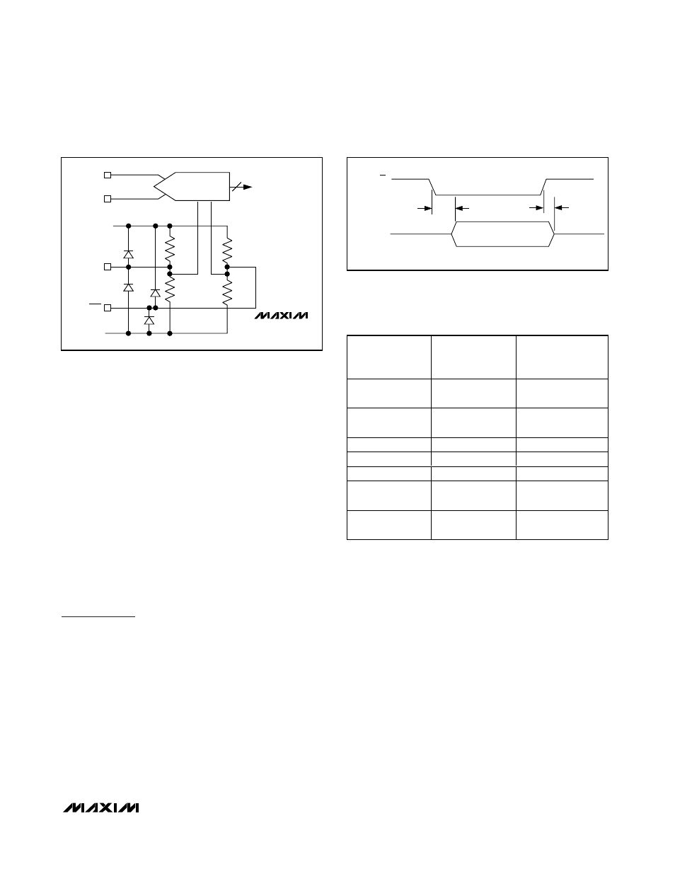
Figure 4. Simplified Clock Input Circuit
OUTPUT
DATA D11–D0
OE
t
BD
t
BE
HIGH-Z
HIGH-Z
VALID DATA
Figure 5. Output Enable Timing
DIFFERENTIAL
INPUT
VOLTAGE*
DIFFERENTIAL
INPUT
OFFSET BINARY
V
REF
✕
2047/2048
+FULL SCALE -
1LSB
1111 1111 1111
V
REF
✕
2046/2048
+FULL SCALE -
2LSB
1111 1111 1110
V
REF
✕
1/2048
+1 LSB
1000 0000 0001
0
Bipolar Zero
1000 0000 0000
-V
REF ✕
1/2048
-1 LSB
0111 1111 1111
-V
REF
✕
2046/2048
-FULL SCALE
+1 LSB
0000 0000 0001
-V
REF
✕
2047/2048
-FULL SCALE
0000 0000 0000
Table 1. MAX1422 Output Code For
Differential Inputs
*V
REF
= V
REFP
- V
REFN