Rainbow Electronics MAX3079E User Manual
Page 2
MAX3070E–MAX3079E
+3.3V, ±15kV ESD-Protected, Fail-Safe,
Hot-Swap, RS-485/RS-422 Transceivers
2
_______________________________________________________________________________________
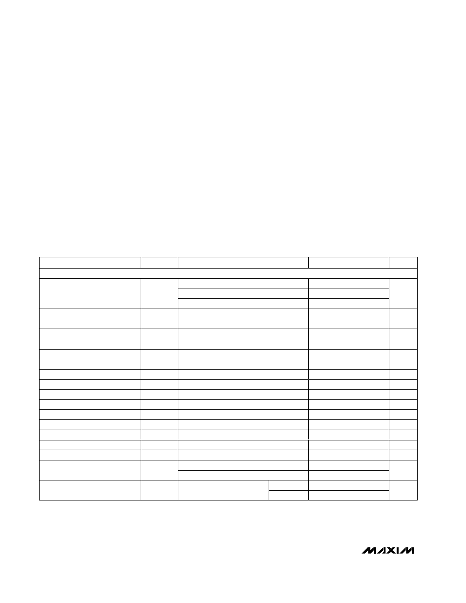
ABSOLUTE MAXIMUM RATINGS
DC ELECTRICAL CHARACTERISTICS
(V
CC
= 3.3V ±10%, T
A
=T
MIN
to T
MAX
, unless otherwise noted. Typical values are at V
CC
= 3.3V and T
A
= +25°C.) (Note 1)
Stresses beyond those listed under “Absolute Maximum Ratings” may cause permanent damage to the device. These are stress ratings only, and functional
operation of the device at these or any other conditions beyond those indicated in the operational sections of the specifications is not implied. Exposure to
absolute maximum rating conditions for extended periods may affect device reliability.
(All voltages referenced to GND)
Supply Voltage (V
CC
).............................................................+6V
Control Input Voltage (RE, DE, SLR,
H/F, TXP, RXP)......................................................-0.3V to +6V
Driver Input Voltage (DI)...........................................-0.3V to +6V
Driver Output Voltage (Z, Y, A, B) .............................-8V to +13V
Receiver Input Voltage (A, B)....................................-8V to +13V
Receiver Input Voltage
Full Duplex (A, B) ..................................................-8V to +13V
Receiver Output Voltage (RO)....................-0.3V to (V
CC
+ 0.3V)
Driver Output Current .....................................................±250mA
Continuous Power Dissipation (T
A
= +70°C)
8-Pin SO (derate 5.88mW/°C above +70°C) .................471mW
8-Pin Plastic DIP (derate 9.09mW/°C above +70°C) .....727mW
14-Pin SO (derate 8.33mW/°C above +70°C) ...............667mW
14-Pin Plastic DIP (derate 10.0mW/°C above +70°C) ...800mW
Operating Temperature Ranges
MAX307_EE_ _ ................................................-40°C to +85°C
MAX307_EA_ _ ..............................................-40°C to +125°C
Junction Temperature ......................................................+150°C
Storage Temperature Range .............................-65°C to +150°C
Lead Temperature (soldering, 10s) .................................+300°C
PARAMETER
SYMBOL
CONDITIONS
MIN
TYP
MAX
UNITS
DRIVER
R
L
= 100
Ω (RS422), Figure 1
2
V
CC
R
L
= 54
Ω (RS485), Figure 1
1.5
V
CC
Differential Driver Output
V
OD
No load
V
CC
V
Change in Magnitude of
Differential Output Voltage
∆V
OD
R
L
= 100
Ω or 54Ω, Figure 1 (Note 2)
0.2
V
Driver Common-Mode Output
Voltage
V
OC
R
L
= 100
Ω or 54Ω, Figure 1
V
CC
/ 2
3
V
Change in Magnitude of
Common-Mode Voltage
∆V
OC
R
L
= 100
Ω or 54Ω, Figure 1 (Note 2)
0.2
V
Input High Voltage
V
IH
DE, DI, RE, TXP, RXP, H/F
2
V
Input Low Voltage
V
IL
DE, DI, RE, TXP, RXP, H/F
0.8
V
Input Hysteresis
V
HYS
DE, DI, RE, TXP, RXP, H/F
100
mV
Input Current
I
IN1
DE, DI, RE
±1
µA
Input Impedance First Transition
DE
1
10
k
Ω
Input Current
I
IN2
TXP, RXP, H/F internal pulldown
10
40
µA
SRL Input High Voltage
V
CC
- 0.4
V
SRL Input Middle Voltage
V
CC
x 0.4 V
CC
x 0.6
V
SRL Input Low Voltage
0.4
V
SRL = V
CC
75
SRL Input Current
SRL = GND
-75
µA
V
IN
= +12V
125
Output Leakage (Y and Z)
Full Duplex
I
O
DE = GND,
V
CC
= GND or 3.6V
V
IN
= -7V
-100
µA