Electrical characteristics (continued) – Rainbow Electronics MAX1126 User Manual
Page 3
MAX1126
Quad, 12-Bit, 40Msps, 1.8V ADC with
Serial LVDS Outputs
_______________________________________________________________________________________
3
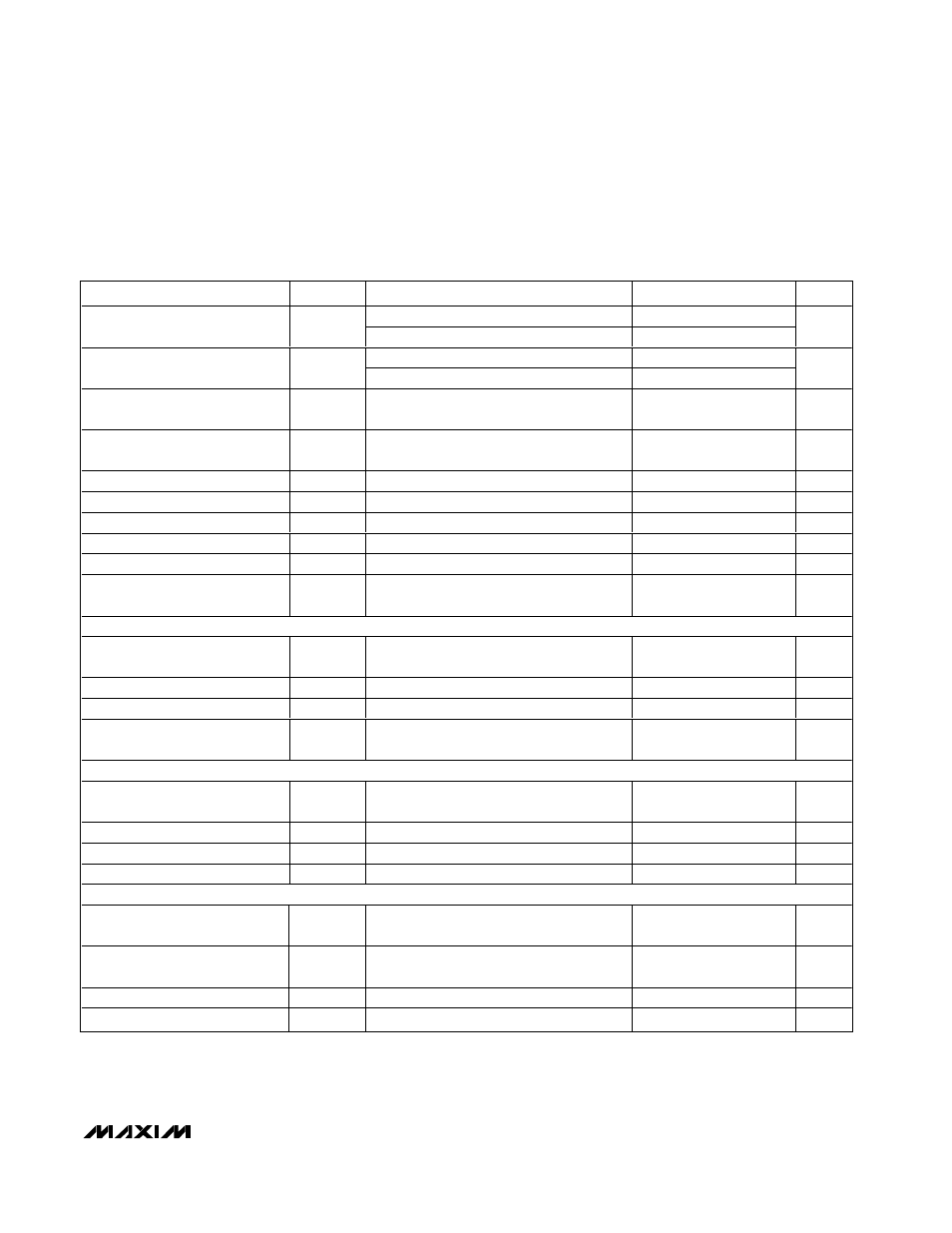
ELECTRICAL CHARACTERISTICS (continued)
(AV
DD
= 1.8V, OV
DD
= 1.8V, CV
DD
= 1.8V, GND = 0, external V
REFIO
= 1.24V, INTREF = AV
DD
, C
REFIO
to GND = 0.1µF,
f
CLK
= 40MHz (50% duty cycle), DT = 0, T
A
= T
MIN
to T
MAX
, unless otherwise noted. Typical values are at T
A
= +25°C.) (Note 1)
PARAMETER
SYMBOL
CONDITIONS
MIN
TYP
MAX
UNITS
f
IN
= 5.3MHz at -0.5dBFS
93.7
Spurious-Free Dynamic Range
(Note 2)
SFDR
f
IN
= 19.3MHz at -0.5dBFS, T
A
≥
+25°C
77.3
89
dBc
f
IN
= 5.3MHz at -0.5dBFS
-91.5
Total H ar m oni c D i stor ti on ( N ote 2)
THD
f
IN
= 19.3MHz at -0.5dBFS, T
A
≥
+25°C
-88.7
-76.3
dBc
Inter m od ul ati on D i stor ti on
IMD
f
1
= 12.40125MHz at -6.5dBFS,
f
2
= 13.60125MHz at -6.5dBFS ( N ote 2)
87.0
dBc
Third-Order Intermodulation
IM3
f
1
= 12.40125MHz at -6.5dBFS,
f
2
= 13.60125MHz at -6.5dBFS ( N ote 2)
89.3
dBc
Aperture Jitter
t
AJ
(Note 2)
<0.4
ps
RMS
Aperture Delay
t
AD
(Note 2)
1
ns
Small-Signal Bandwidth
SSBW
Input at -20dBFS (Notes 2 and 4)
100
MHz
Full-Power Bandwidth
LSBW
Input at -0.5dBFS (Notes 2 and 4)
100
MHz
Output Noise
IN_P = IN_N
0.35
LSB
RMS
Overdrive Recovery Time
t
OR
R
S
= 25
Ω
, C
S
= 50pF
1
Clock
cycles
INTERNAL REFERENCE (
INTREF
= GND, bypass REFIO to GND with 0.1µF)
INTREF Internal Reference Mode
Enable Voltage
(Note 5)
0.1
V
INTREF Low-Leakage Current
200
µA
REFIO Output Voltage
V
REFIO
1.18
1.24
1.30
V
Reference Temperature
Coefficient
TC
REFIO
100
ppm/°C
EXTERNAL REFERENCE (
INTREF
= AV
DD
)
INTREF External Reference Mode
Enable Voltage
(Note 5)
AV
DD
-
0.1V
V
INTREF High-Leakage Current
200
µA
REFIO Input Voltage Range
1.24
V
REFIO Input Current
I
REFIO
<1
µA
CLOCK INPUT (CLK)
Input High Voltage
V
CLKH
0.8 x
CV
DD
V
Input Low Voltage
V
CLKL
0.2 x
CV
DD
V
Clock Duty Cycle
50
%
Clock Duty-Cycle Tolerance
±30
%