Typical operating characteristics (continued), Pin description – Rainbow Electronics MAX1126 User Manual
Page 14
MAX1126
Quad, 12-Bit, 40Msps, 1.8V ADC with
Serial LVDS Outputs
14
______________________________________________________________________________________
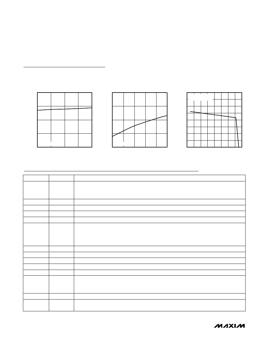
Typical Operating Characteristics (continued)
(AV
DD
= 1.8V, OV
DD
= 1.8V, CV
DD
= 1.8V, GND = 0, external V
REFIO
= 1.24V, INTREF = AV
DD
, differential input at -0.5dBFS,
f
CLK
= 40MHz (50% duty cycle), DT = low, C
LOAD
= 10pF, T
A
= +25°C, unless otherwise noted.)
INTERNAL REFERENCE VOLTAGE
vs. SUPPLY VOLTAGE
SUPPLY VOLTAGE (V)
V
REFIO
(V)
2.0
1.9
1.8
1.236
1.237
1.238
1.239
1.235
1.7
2.1
MAX1126 toc34
AV
DD
= OV
DD
INTERNAL REFERENCE VOLTAGE
vs. TEMPERATURE
TEMPERATURE (°C)
V
REFIO
(V)
60
35
10
-15
1.23
1.24
1.25
1.26
1.22
-40
85
MAX1126 toc35
AV
DD
= OV
DD
INTERNAL REFERENCE VOLTAGE
vs. REFERENCE LOAD CURRENT
I
REFIO
(µA)
V
REFIO
(V)
300
200
-300 -200 -100
0
100
1.05
1.10
1.15
1.20
1.25
1.30
1.35
1.40
1.00
-400
400
MAX1126 toc36
NEGATIVE CURRENT
FLOWS INTO REFIO
PIN
NAME
FUNCTION
1, 4, 7, 11,
14, 17, 22,
24, 65, 68
GND
Ground. Connect all GND pins to the same potential.
2
IN0P
Channel 0 Positive Analog Input
3
IN0N
Channel 0 Negative Analog Input
5
IN1P
Channel 1 Positive Analog Input
6
IN1N
Channel 1 Negative Analog Input
8, 9, 10, 18,
20, 25, 26,
27, 58–62
AV
DD
Analog Power Input. Connect AV
DD
to a 1.7V to 1.9V power supply. Bypass each AV
DD
to GND with
a 0.1µF capacitor as close to the device as possible. Bypass the AV
DD
power plane to the GND
ground plane with a bulk ≥2.2µF capacitor as close to the device as possible. Connect all AV
DD
pins
to the same potential.
12
IN2P
Channel 2 Positive Analog Input
13
IN2N
Channel 2 Negative Analog Input
15
IN3P
Channel 3 Positive Analog Input
16
IN3N
Channel 3 Negative Analog Input
19
I.C.
Internally Connected. Do not connect.
21
CV
DD
Clock Power Input. Connect CV
DD
to a 1.7V to 3.6V supply. Bypass CV
DD
to GND with a 0.1µF
capacitor in parallel with a ≥2.2µF capacitor. Install the bypass capacitors as close to the device as
possible.
23
CLK
Single-Ended CMOS Clock Input
28
DT
Double Termination Select Input. Drive DT high to select the internal 100
Ω
termination between the
differential output pairs. Drive DT low to select no internal output termination.
Pin Description