System timing requirements – Rainbow Electronics MAX1126 User Manual
Page 19
MAX1126
Quad, 12-Bit, 40Msps, 1.8V ADC with
Serial LVDS Outputs
______________________________________________________________________________________
19
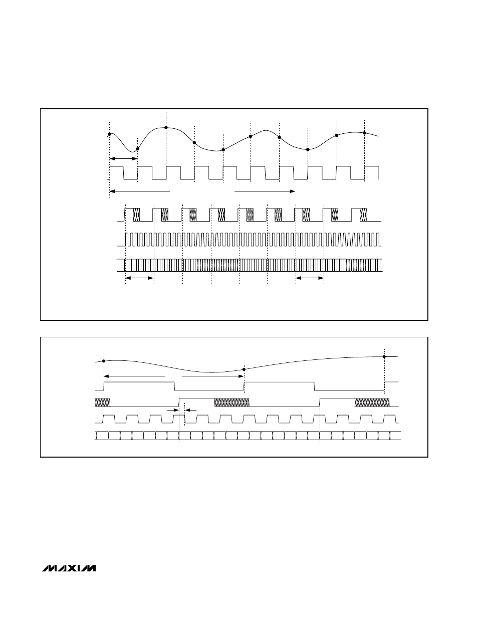
System Timing Requirements
Figure 3 shows the relationship between the analog
inputs, input clock, frame alignment output, serial clock
output, and serial data output. The differential analog
input (IN_P and IN_N) is sampled on the rising edge of
the CLK signal and the resulting data appears at the
digital outputs 6.5 clock cycles later. Figure 4 provides
a detailed, two-conversion timing diagram of the rela-
tionship between the inputs and the outputs.
Clock Output (CLKOUTP, CLKOUTN)
The MAX1126 provides a differential clock output that
consists of CLKOUTP and CLKOUTN. As shown in
Figure 4, the serial output data is clocked out of the
MAX1126 on both edges of the clock output. The fre-
quency of the output clock is 6 times the frequency
of CLK.
OUTPUT
DATA FOR
SAMPLE
N - 6
OUTPUT
DATA FOR
SAMPLE N
*DUTY CYCLE VARIES DEPENDING ON INPUT CLOCK FREQUENCY.
CLK
N
N + 2
N + 1
N + 3
N + 4
N + 5
N + 6
N + 7
N + 8
N + 9
6.5 CLOCK-CYCLE DATA LATENCY
t
SAMPLE
(V
IN_P
-
V
IN_N
)
(V
FRAMEP
-
V
FRAMEN
)*
(V
CLKOUTP
-
V
CLKOUTN
)
(V
OUT_P
-
V
OUT_N
)
Figure 3. Global Timing Diagram
N
N + 2
N + 1
*DUTY CYCLE DEPENDS ON INPUT CLOCK FREQUENCY.
t
CF
(V
IN_P
- V
IN_N
)
CLK
(V
FRAMEP
-
V
FRAMEN
)
(V
CLKOUTP
-
V
CLKOUTN
)
(V
OUT_P
-
V
OUT_N
)
D5
N-7
D6
N-7
D7
N-7
D8
N-7
D9
N-7
D10
N-7
D11
N-7
D0
N-6
D1
N-6
D2
N-6
D3
N-6
D4
N-6
D5
N-6
D6
N-6
D7
N-6
D8
N-6
D9
N-6
D10
N-6
D11
N-6
D0
N-5
D1
N-5
D2
N-5
D3
N-5
D4
N-5
D5
N-5
D6
N-5
t
SAMPLE
Figure 4. Detailed Two-Conversion Timing Diagram