Typical application circuit, Layout considerations – Rainbow Electronics MAX3622 User Manual
Page 8
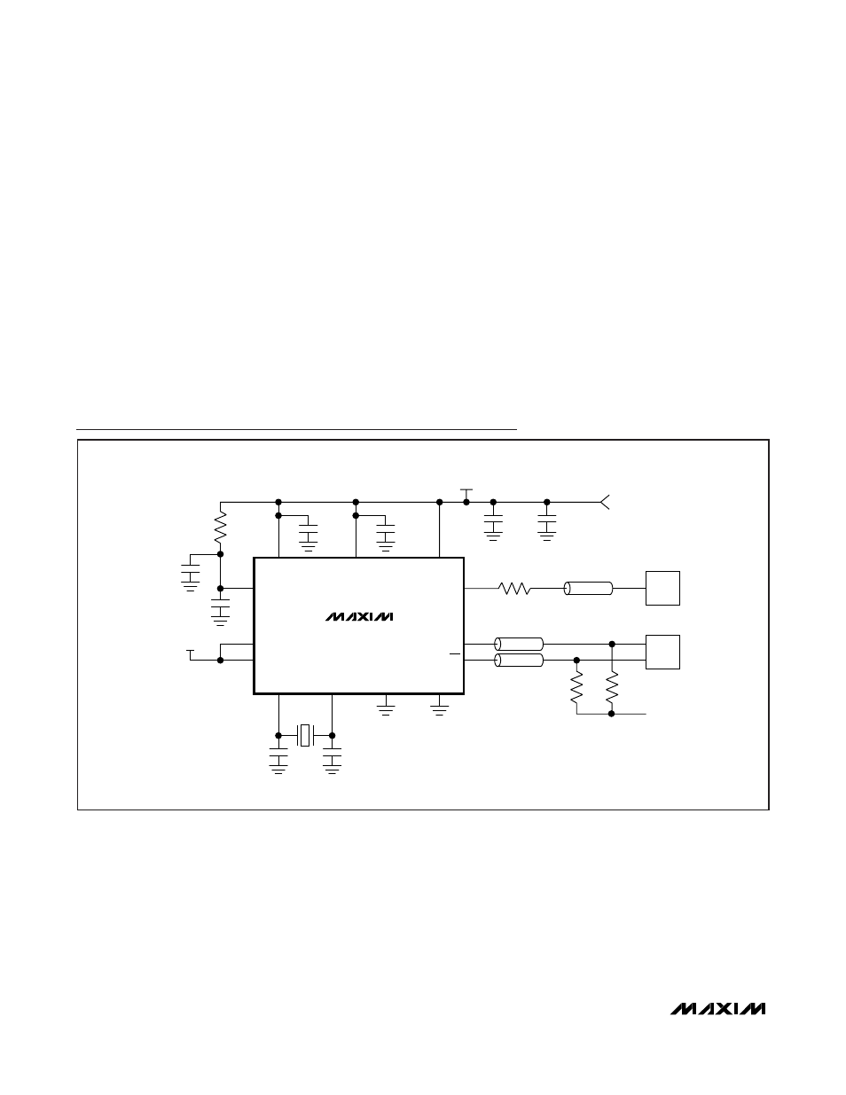
Layout Considerations
The inputs and outputs are critical paths for the
MAX3622, and care should be taken to minimize dis-
continuities on these transmission lines. Here are some
suggestions for maximizing the MAX3622’s perfor-
mance:
• An uninterrupted ground plane should be posi-
tioned beneath the clock I/Os.
• Supply and ground pin vias should be placed
close to the IC and the input/output interfaces to
allow a return current path to the MAX3622 and the
receive devices.
• Supply decoupling capacitors should be placed
close to the MAX3622 supply pins.
• Maintain 100
Ω differential (or 50Ω single-ended)
transmission line impedance out of the MAX3622.
• Use good high-frequency layout techniques and a
multilayer board with an uninterrupted ground
plane to minimize EMI and crosstalk.
Refer to the MAX3622 Evaluation Kit for more information.
MAX3622
Low-Jitter, Precision Clock Generator
with Two Outputs
8
_______________________________________________________________________________________
MAX3622
V
CCA
QAC_OE
QB_OE
QA_C
X_OUT
X_IN
GNDO_A
GND
V
CC
V
CCO_B
V
DDO_A
10.5
Ω
0.01
μF
0.1
μF
V
CC
36
Ω
Z
0
= 50
Ω
ASIC
125MHz
QB
50
Ω
Z
0
= 50
Ω
QB
Z
0
= 50
Ω
ASIC
50
Ω
156.25MHz
(V
CC
- 2V)
10
μF
0.1
μF
25MHz
(C
L
= 18pF)
33pF
27pF
0.01
μF
0.1
μF
+3.3V
±5%
V
CC
Typical Application Circuit