Max3622, Pin description, Detailed description – Rainbow Electronics MAX3622 User Manual
Page 5
MAX3622
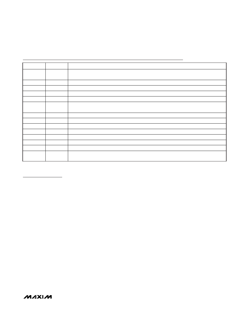
Pin Description
PIN
NAME
FUNCTION
1 QAC_OE
LVCMOS/LVTTL Input. Enables/disables QA_C clock output. Connect pin high to enable QA_C.
Connect low to set QA_C to a high-impedance state. Has internal 50k
input impedance.
2
GNDO_A
Ground for QA_C Output. Connect to supply ground.
3
QA_C
LVCMOS Clock Output
4 V
DDO_A
Power Supply for QA_C Clock Output. Connect to +3.3V.
5, 6
RES1, RES2 Reserved. Do not connect.
7 V
CCA
Analog Power Supply for the VCO. Connect to +3.3V. For additional power-supply noise filtering,
this pin can connect to V
CC
through 10.5
as shown in Figure 2 (requires V
CC
= +3.3V ±5%).
8 V
CC
Core Power Supply. Connect to +3.3V.
9, 15
GND
Supply Ground
10 X_OUT
Crystal
Oscillator
Output
11
X_IN
Crystal Oscillator Input
12 V
CCO_B
Power Supply for QB Clock Output. Connect to +3.3V.
13
QB
LVPECL, Inverting Clock Output
14
QB
LVPECL, Noninverting Clock Output
16 QB_OE
LVCMOS/LVTTL Input. Enables/disables QB clock output. Connect pin high to enable LVPECL clock
output QB. Connect low to set QB to a logic 0. Has internal 50k
input impedance.
Low-Jitter, Precision Clock Generator
with Two Outputs
_______________________________________________________________________________________
5
Detailed Description
The MAX3622 is a low-jitter clock generator designed
to operate at Ethernet frequencies. It consists of an on-
chip crystal oscillator, PLL, LVCMOS output buffer, and
an LVPECL output buffer. Using a 25MHz crystal as a
reference, the internal PLL generates a high-frequency
output clock with excellent jitter performance.
Crystal Oscillator
An integrated oscillator provides the low-frequency ref-
erence clock for the PLL. This oscillator requires a
25MHz crystal connected between X_IN and X_OUT.
PLL
The PLL takes the signal from the crystal oscillator and
synthesizes a low-jitter, high-frequency clock. The PLL
contains a phase-frequency detector (PFD), a lowpass
filter, and a voltage-controlled oscillator (VCO). The
VCO output is connected to the PFD input through a
feedback divider. The PFD compares the reference fre-
quency to the divided-down VCO output (f
VCO
/25) and
generates a control signal that keeps the VCO locked
to the reference clock. The high-frequency VCO output
clock is sent to the output dividers. To minimize noise-
induced jitter, the VCO supply (V
CCA
) is isolated from
the core logic and output buffer supplies.
Output Dividers
The output dividers are set to divide-by-five for the
LVCMOS output QA_C and divide-by-four for the
LVPECL output QB.
LVPECL Driver
The differential PECL buffer (QB) is designed to drive
transmission lines terminated with 50
Ω to V
CC
- 2.0V.
The output goes to a logic 0 when disabled.
LVCMOS Driver
QA_C, the LVCMOS output, is designed to drive a sin-
gle-ended high-impedance load. This output goes to a
high-impedance state when disabled.
Reset Logic/POR
During power-on, the power-on reset (POR) signal is
generated to synchronize all dividers.