Rainbow Electronics MAX1706 User Manual
Page 2
MAX1705/MAX1706
1- to 3-Cell, High-Current, Low-Noise,
Step-Up DC-DC Converters with Linear Regulator
2
_______________________________________________________________________________________
ABSOLUTE MAXIMUM RATINGS
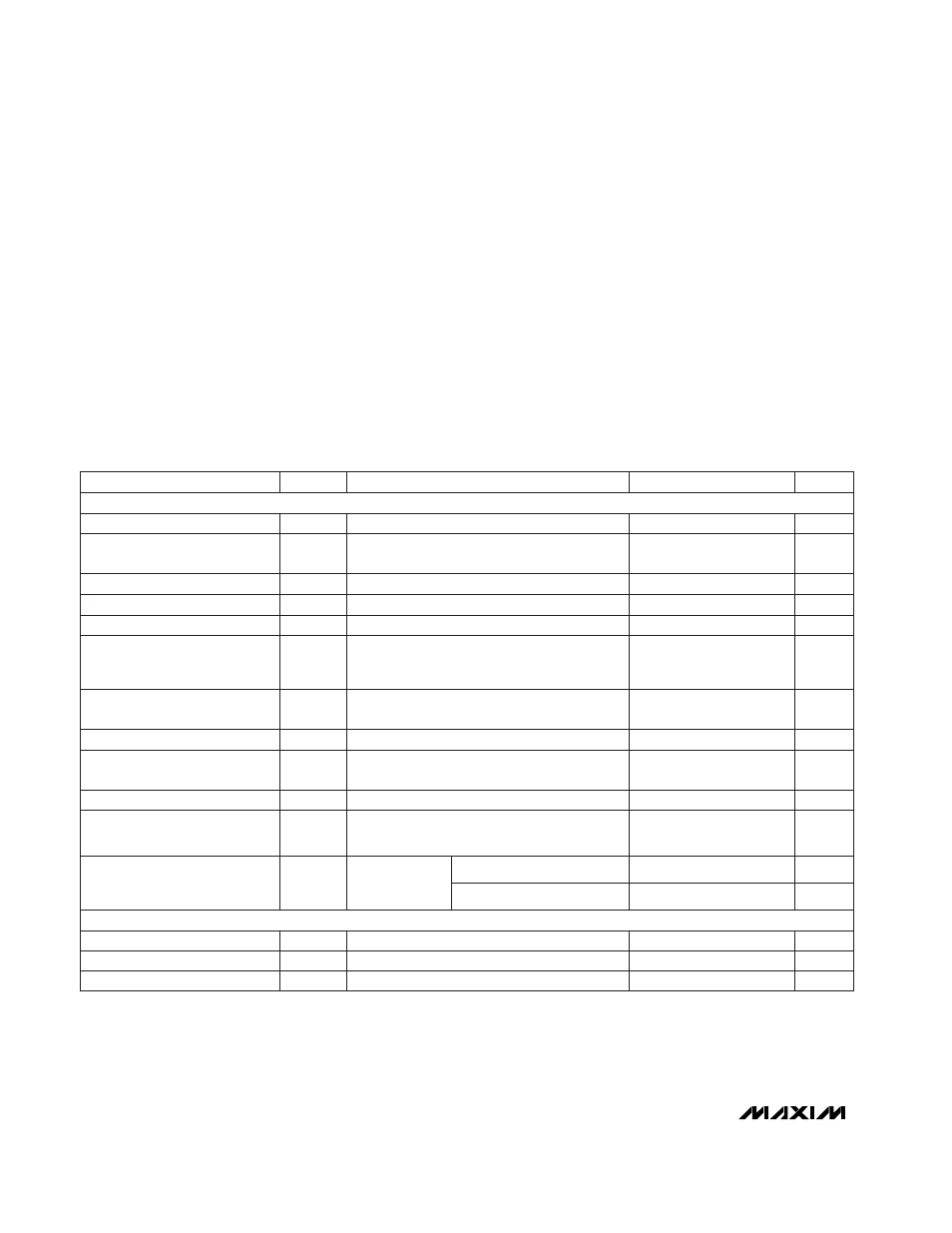
ELECTRICAL CHARACTERISTICS
(V
OUT
= V
POUT
= V
LBP
= 3.6V, CLK/SEL = FB = LBN = LBO = ONA =
ONB = TRACK = GND, REF = open (bypassed with 0.22µF),
LX = open,
T
A
= 0°C to +85°C,
unless otherwise noted. Typical values are at T
A
= +25°C.)
Stresses beyond those listed under “Absolute Maximum Ratings” may cause permanent damage to the device. These are stress ratings only, and functional
operation of the device at these or any other conditions beyond those indicated in the operational sections of the specifications is not implied. Exposure to
absolute maximum rating conditions for extended periods may affect device reliability.
ONA, ONB, FBLDO, OUT, POUT to GND...................-0.3V to 6V
PGND to GND.....................................................................±0.3V
POUT to OUT ......................................................................±0.3V
LX to PGND ............................................-0.3V to (V
POUT
+ 0.3V)
CLK/SEL, REF, FB, TRACK, LDO,
LBN, LBP, LBO to GND.......................-0.3V to (V
OUT
+ 0.3V)
LDO Short Circuit .......................................................Continuous
Continuous Power Dissipation (T
A
= +70°C)
QSOP (derate 8.70mW/°C above +70°C) ...................696mW
Operating Temperature Range ...........................-40°C to +85°C
Junction Temperature ......................................................+150°C
Storage Temperature Range .............................-65°C to +160°C
Lead Temperature (soldering, 10sec) .............................+300°C
CLK/SEL = OUT
-1µA < I
REF
< 50µA
(Note 1)
I
REF
= 0µA
CLK/SEL = GND, V
FB
= V
FBLDO
= 1.5V,
no load
ONA = GND, ONB = OUT, measure I
OUT
(Note 2)
V
POUT
= V
OUT
= 1.5V
V
FB
= 1.5V
MAX1705, 0A
≤
I
LX
≤
0.5A;
MAX1706, 0A
≤
I
LX
≤
0.25A;
CLK/SEL = OUT
TRACK = V
LDO
> 2.3V
CLK/SEL = OUT
CONDITIONS
mV
4
15
Reference Load Regulation
V
1.238
1.250
1.262
Reference Output Voltage
µA
180
360
I
OUT
Supply Current in
Low-Noise Mode
V
1.219
1.233
1.247
FB Regulation Voltage
V
0.7
Minimum Operating Battery
Voltage
µA
100
190
I
OUT
Supply Current in
Low-Power Mode
µA
1
20
I
OUT
Supply Current in Shutdown
V
2.00
2.15
2.30
Start-Up to Normal Mode
Transition Voltage
kHz
40
150
300
f
LX
Frequency in Start-Up Mode
nA
0.01
50
FB Input Current
V
2.5
5.5
OUT Adjust Range
%
0.65
1.25
Load Regulation
V
V
LDO
V
LDO
V
LDO
+ 0.2
+ 0.3
+ 0.4
OUT Voltage in Track Mode
UNITS
MIN
TYP
MAX
SYMBOL
PARAMETER
T
A
= +25°C, I
LOAD
< 1mA, Figure 2
V
0.9
1.1
Minimum Start-Up Voltage
2.5V < V
OUT
< 5.5V
mV
0.2
5
Reference Supply Regulation
DC-DC CONVERTER
REFERENCE
V
FB
= V
FBLDO
= 1.5V, no load
FB = GND (LX switching)
2.1
mA