Pin description – Rainbow Electronics MAX3629 User Manual
Page 8
MAX3629
+3.3V, Low-Jitter, Precision Clock Generator
with Multiple Outputs
8
_______________________________________________________________________________________
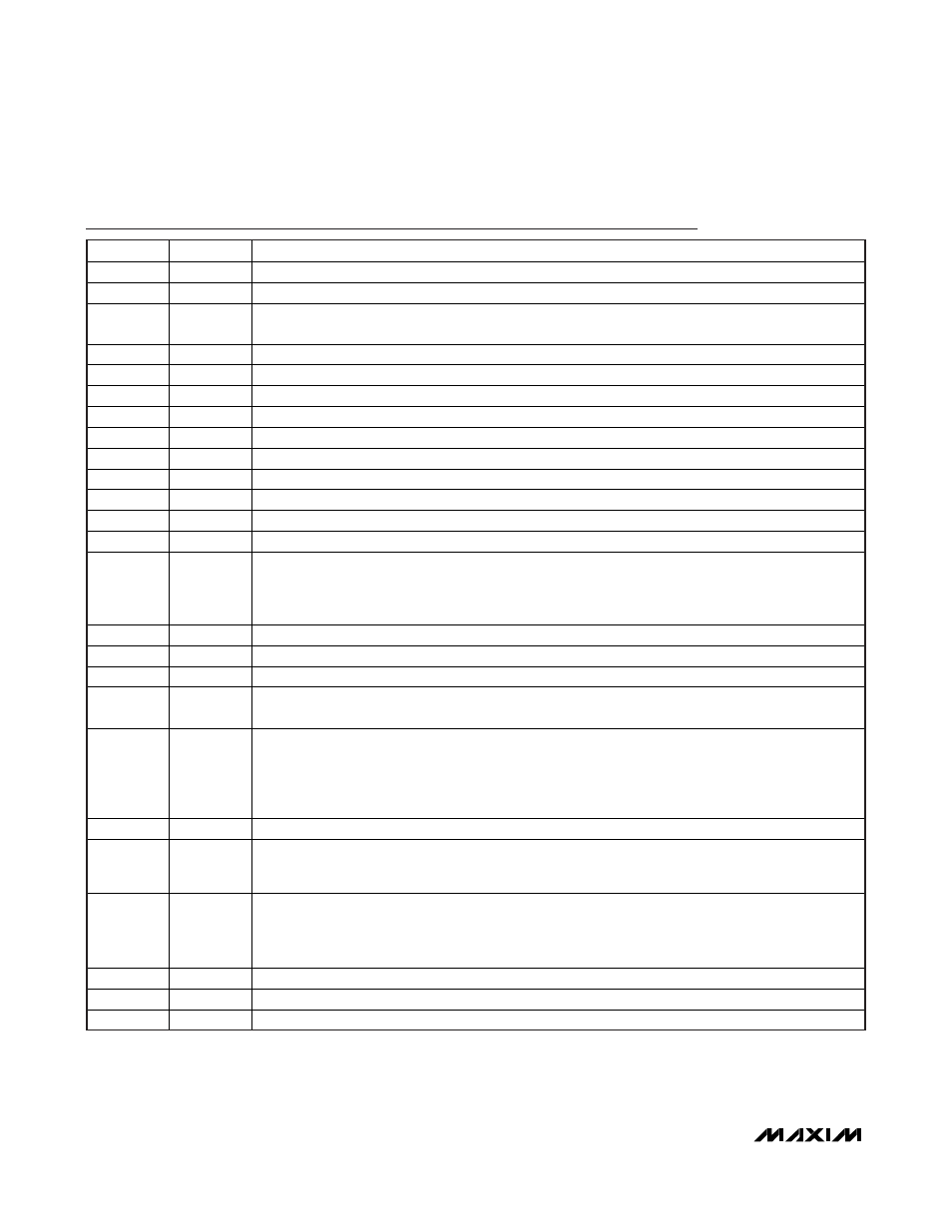
Pin Description
PIN
NAME
FUNCTION
1
Q0
LVDS, Noninverting Clock Output
2
Q0
LVDS, Inverting Clock Output
3, 9, 17, 21,
32
GND Supply
Ground
4
Q1
LVDS, Noninverting Clock Output
5
Q1
LVDS, Inverting Clock Output
6, 12
V
DDO_DIFF
Power Supply for Q0, Q1, Q2, Q3, and Q4 Clock Outputs. Connect to +3.3V.
7
Q2
LVDS, Noninverting Clock Output
8
Q2
LVDS, Inverting Clock Output
10
Q3
LVDS, Noninverting Clock Output
11
Q3
LVDS, Inverting Clock Output
13
Q4
LVDS, Noninverting Clock Output
14
Q4
LVDS, Inverting Clock Output
15
RESERVED Reserved. Connect to GND.
16 FSELB
Three-State LVCMOS/LVTTL Input. Controls the Q1 to Q7 output divider. When connected to logic-
low, the output frequency is 125MHz. When connected to logic-high, the output frequency is
156.25MHz. When left open (high-Z), the output frequency is 312.5MHz. For Q5 to Q7 LVCMOS
outputs, the output specification is only valid up to 160MHz.
18, 20, 22
Q5, Q6, Q7 LVCMOS Clock Output
19, 23
V
DDO_SE
Power Supply for Q5, Q6, and Q7 Clock Outputs. Connect to +3.3V.
24 RESERVED
Reserved.
Leave
open.
25 V
DDA
Analog Power Supply for the VCO. Connect to +3.3V. For additional power-supply noise filtering, this
pin can connect to V
DD
through a 10.5
resistor as shown in Figure 4.
26
PLL_BP
Three-State LVCMOS/LVTTL Input (Active Low). When connected to logic-high, the PLL locks to the
crystal interface (25MHz typical at X_IN and X_OUT). When left open (high-Z), the PLL locks to the
OSC_IN input (25MHz typical). When connected to logic-low, the PLL is bypassed and the OSC_IN
input is selected. When bypass mode is selected, the VCO/PLL is disabled to save power and
eliminate intermodulation spurs.
27 V
DD
Power Supply for Digital Part of the Chip. Connect to +3.3V.
28 FSELA
Three-State LVCMOS/LVTTL Input. Controls the Q0 output divider. When connected to logic-low, the
output frequency is 125MHz. When connected to logic-high, the output frequency is 156.25MHz.
When left open (high-Z), the output frequency is 312.5MHz.
29 OSC_IN
LVCMOS Input. Self-biased to allow AC- or DC-coupling. When
PLL_BP is open, the OSC_IN input
frequency should be 25MHz. When the PLL is in bypass mode (
PLL_BP = low), the OSC_IN input
frequency can be between 20MHz and 320MHz. When
PLL_BP is high, the OSC_IN should be
disconnected.
30
X_IN
Crystal Oscillator Input
31 X_OUT
Crystal
Oscillator
Output
—
EP
Exposed Pad. Connect to GND for proper electrical and thermal performance.