Electrical characteristics (continued) – Rainbow Electronics MAX3629 User Manual
Page 4
MAX3629
+3.3V, Low-Jitter, Precision Clock Generator
with Multiple Outputs
4
_______________________________________________________________________________________
ELECTRICAL CHARACTERISTICS (continued)
(V
DD
= +3.0V to +3.6V, T
A
= 0°C to +70°C, unless otherwise noted. Typical values are at V
DD
= +3.3V, T
A
= +25°C, unless otherwise
noted. When using X_IN, X_OUT input, no signal is applied at OSC_IN. When PLL is enabled, PLL_BP = high-Z or high. When PLL is
bypassed, PLL_BP = low.) (Note 1)
PARAMETER
SYMBOL
CONDITIONS
MIN
TYP
MAX
UNITS
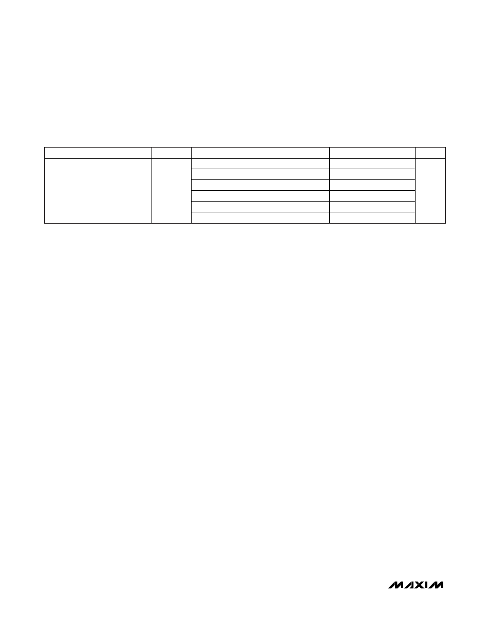
f
=
100Hz
-115
f
=
1kHz
-124
f
=
10kHz
-126
f = 100kHz
-130
f
=
1MHz
-144
LVCMOS Clock Output SSB
Phase Noise at 125MHz
(Note 14)
f
>
10MHz
-151
dBc/Hz
Note 1:
A series resistor of up to 10.5
Ω is allowed between V
DD
and V
DDA
for filtering supply noise when system power-supply tol-
erance is V
DD
= 3.3V ±5%. See Figure 4.
Note 2:
All outputs unloaded.
Note 3:
The current when an LVDS output is shorted to ground is the steady-state current after the detection circuitry has settled. It
is expected that the LVDS output short to ground condition is short-term only.
Note 4:
Measured with OSC_IN input with 50% duty cycle.
Note 5:
Measured with a series resistor of 33
Ω to a load capacitance of 3.0pF. See Figure 2.
Note 6:
The OSC_IN input can be DC- or AC-coupled.
Note 7:
Must be within the absolute maximum rating of V
DD
+ 0.3V.
Note 8:
AC characteristics of LVCMOS outputs (Q5, Q6, and Q7) are only guaranteed up to 160MHz.
Note 9:
Measured with 25MHz crystal (with OSC_IN left open).
Note 10: Measured with 25MHz reference clock applied to OSC_IN.
Note 11: Measured at 125MHz output with 40mV
P-P
sinusoidal signal on the supply at 100kHz. Measured with a 10.5
Ω resistor
between V
DD
and V
DDA
.
Note 12: Parameter calculated based on PSNR.
Note 13: Measurement includes XTAL oscillator feedthrough, crosstalk, intermodulation spurs, etc.
Note 14: Measured with 25MHz XTAL oscillator.