Chip information, Package information – Rainbow Electronics MAX3629 User Manual
Page 12
MAX3629
+3.3V, Low-Jitter, Precision Clock Generator
with Multiple Outputs
Maxim cannot assume responsibility for use of any circuitry other than circuitry entirely embodied in a Maxim product. No circuit patent licenses are
implied. Maxim reserves the right to change the circuitry and specifications without notice at any time.
12 ____________________Maxim Integrated Products, 120 San Gabriel Drive, Sunnyvale, CA 94086 408-737-7600
© 2009 Maxim Integrated Products
Maxim is a registered trademark of Maxim Integrated Products, Inc.
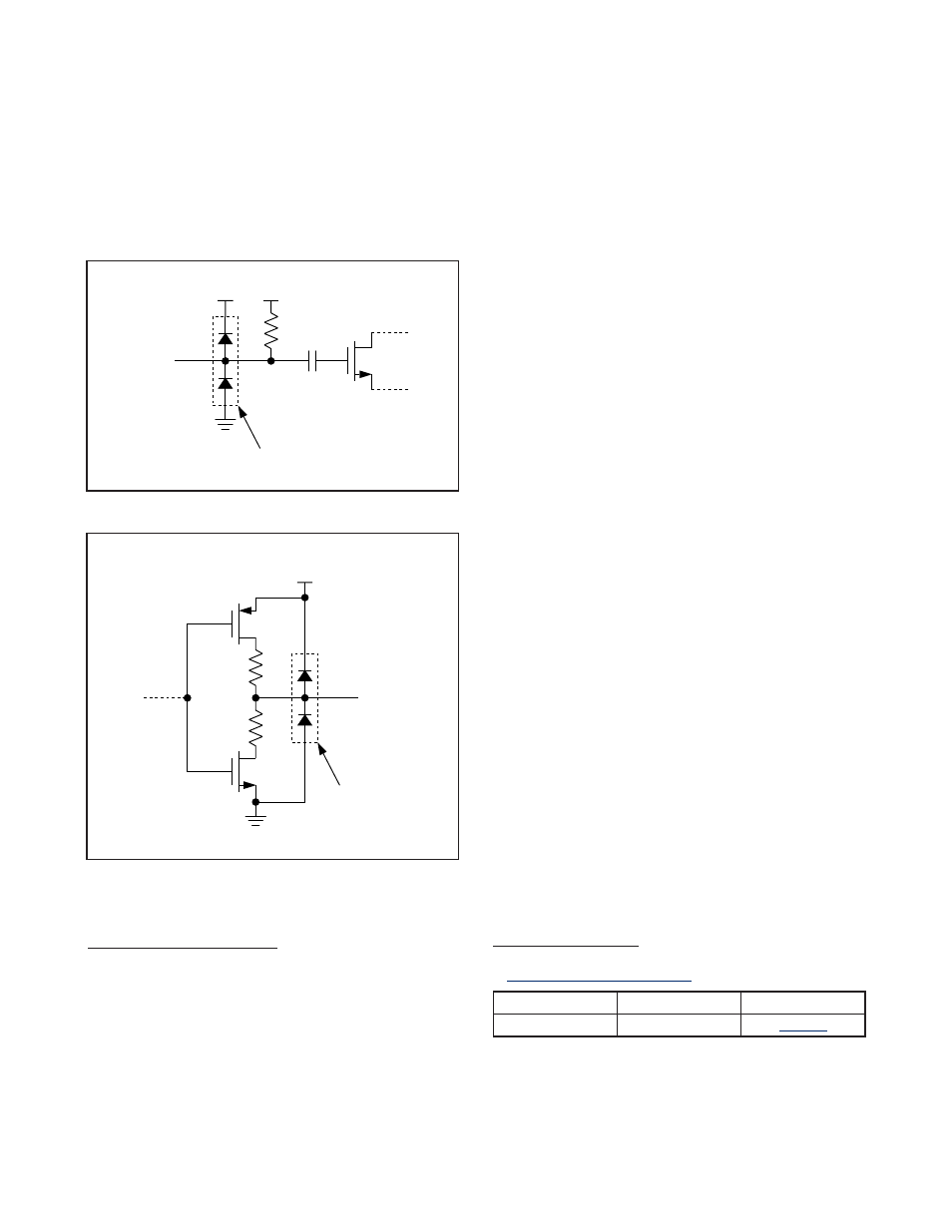
Interface Models
Figures 7 and 8 show examples of interface models.
Layout Considerations
The inputs and outputs are the most critical paths for
the MAX3629 and great care should be taken to mini-
mize discontinuities on these transmission lines
between the connector and the IC. Here are some sug-
gestions for maximizing the performance of the
MAX3629:
• An uninterrupted ground plane should be posi-
tioned beneath the clock outputs. The ground
plane under the crystal should be removed to mini-
mize capacitance.
• Ground pin vias should be placed close to the IC
and the input/output interfaces to allow a return
current path to the MAX3629 and the receive
devices.
• Supply decoupling capacitors should be placed
close to the supply pins, preferably on the same
layer as the MAX3629.
• Take care to isolate crystal input traces from the
MAX3629 outputs.
• The crystal, trace, and two external capacitors
should be placed on the board as close as possi-
ble to the X_IN and X_OUT pins to reduce
crosstalk and active signals into the oscillator.
• Maintain 100
Ω differential (or 50Ω single-ended)
transmission line impedance into and out of the
part.
• Use good high-frequency layout techniques and
multilayer boards with an uninterrupted ground
plane to minimize EMI and crosstalk.
Refer to the MAX3629 evaluation kit for more information.
Exposed-Pad Package
The exposed pad on the 32-pin TQFN package pro-
vides a very low inductance path for return current trav-
eling to the PCB ground plane. The pad is also
electrical ground on the MAX3629 and must be sol-
dered to the circuit board ground for proper electrical
performance.
180k
Ω
1.4V
ESD
STRUCTURES
OSC_IN
V
DD
Figure 7. Simplified OSC_IN Pin Circuit Schematic
10
Ω
10
Ω
ESD
STRUCTURES
Q5 TO Q7
V
DDO_SE
Figure 8. Simplified LVCMOS Output Circuit Schematic
Chip Information
PROCESS: BiCMOS
Package Information
For the latest package outline information and land patterns, go
to
www.maxim-ic.com/packages
.
PACKAGE TYPE
PACKAGE CODE
DOCUMENT NO.
32 TQFN-EP
T3255+5