Rainbow Electronics MAX3629 User Manual
General description, Applications, Features
MAX3629
+3.3V, Low-Jitter, Precision Clock Generator
with Multiple Outputs
________________________________________________________________
Maxim Integrated Products
1
19-4467; Rev 0; 2/09
For pricing, delivery, and ordering information, please contact Maxim Direct at 1-888-629-4642,
or visit Maxim’s website at www.maxim-ic.com.
General Description
The MAX3629 is a low-jitter precision clock generator
optimized for network applications. The device inte-
grates a crystal oscillator and a phase-locked loop
(PLL) to generate high-frequency clock outputs for
Ethernet applications.
Maxim’s proprietary PLL design features ultra-low jitter
(0.4ps
RMS
) and excellent power-supply noise rejection
(PSNR), minimizing design risk for network equipment.
The MAX3629 contains five LVDS outputs and three
LVCMOS outputs. The output frequencies are selec-
table among 125MHz, 156.25MHz, and 312.5MHz by
pin control.
Applications
Ethernet Networking Equipment
Features
♦ Crystal Oscillator Interface: 25MHz
♦ OSC_IN Interface:
PLL Enabled: 25MHz
PLL Disabled: 20MHz to 320MHz
♦ Outputs:
One LVDS Output at 125MHz/156.25MHz/
312.5MHz (Selectable with FSELA)
Four LVDS Outputs at 125MHz/156.25MHz/
312.5MHz (Selectable with FSELB)
Three LVCMOS Outputs at 125MHz/156.25MHz
(Selectable with FSELB)
♦ Low Phase Jitter: 0.4ps
RMS
(12kHz to 20MHz)
♦ Excellent PSNR
♦ Operating Temperature Range: 0°C to +70°C
THIN QFN-EP
(5mm
×
5mm)
TOP VIEW
29
30
28
27
12
11
13
Q0
Q1
Q1
V
DDO_DIFF
Q2
14
Q0
V
DDO_SE
GND
Q6
RESERVED
V
DDO_SE
Q5
1
2
FSELA
4
5
6
7
23
24
22
20
19
18
OSC_IN
X_IN
Q4
Q4
V
DDO_DIFF
Q3
GND
Q7
3
21
31
10
X_OUT
Q3
32
9
GND
GND
V
DD
26
15
RESERVED
PLL_BP
25
16
FSELB
Q2
GND
8
17
V
DDA
+
*EP
*EXPOSED PAD CONNECTED TO GROUND.
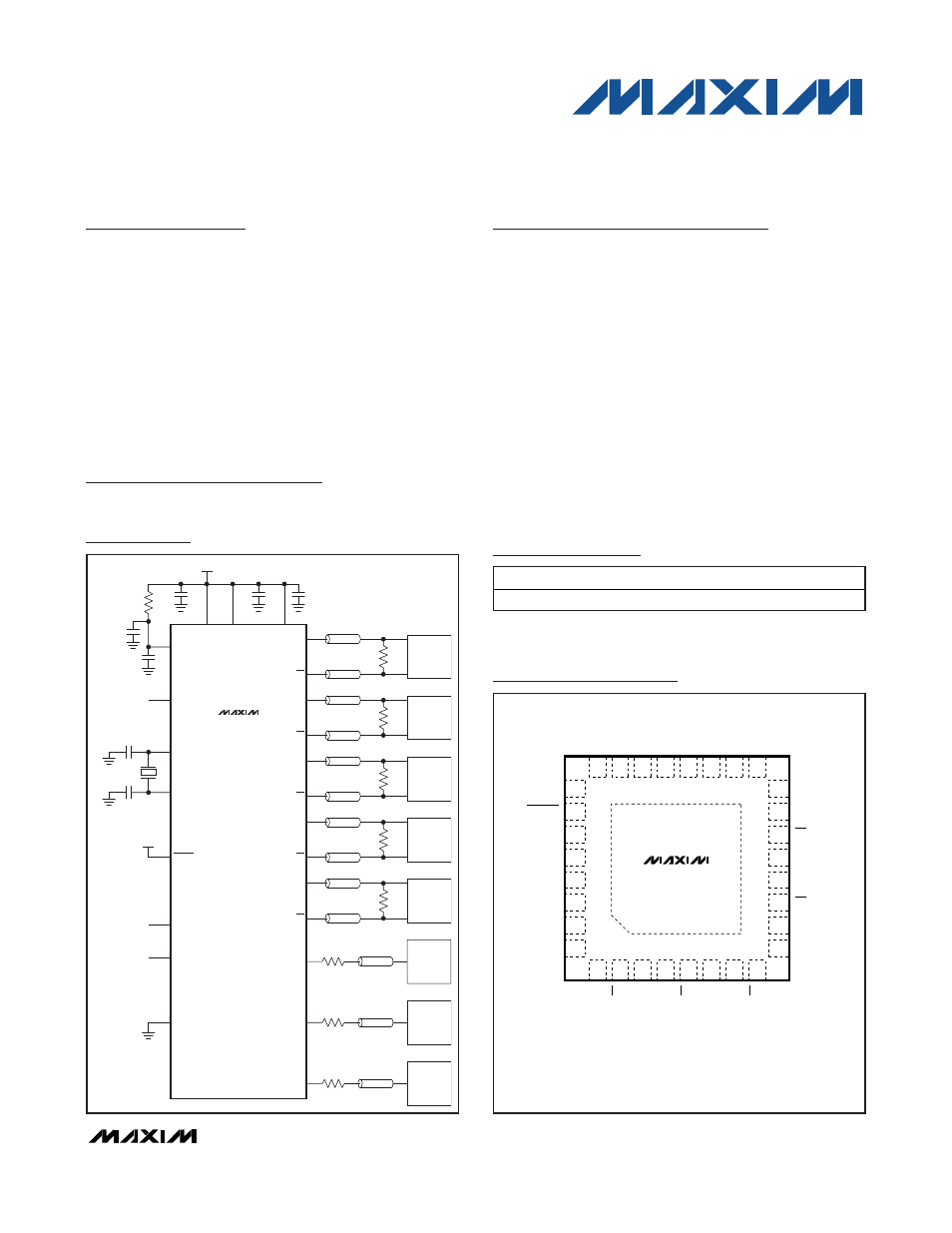
MAX3629
Pin Configuration
Ordering Information
V
DDA
OSC_IN
FSELA
GND, OPEN, OR V
DD
FSELB
GND, OPEN, OR V
DD
GND
PLL_BP
X_OUT
V
DDO_SE
V
DDO_DIFF
V
DD
33pF
X_IN
27pF
25MHz
(C
L
= 18pF)
33
Ω
10.5
Ω
0.1
μF
+3.3V
±5%
Q0
100
Ω
Z
0
= 50
Ω
Q0
Z
0
= 50
Ω
125MHz/156.25MHz/
312.5MHz
125MHz/156.25MHz/
312.5MHz
ASIC
Q1
100
Ω
125MHz/156.25MHz/
312.5MHz
Z
0
= 50
Ω
Q1
Z
0
= 50
Ω
ASIC
Q2
100
Ω
125MHz/156.25MHz/
312.5MHz
Z
0
= 50
Ω
Q2
Z
0
= 50
Ω
ASIC
Q3
100
Ω
125MHz/156.25MHz/
312.5MHz
Z
0
= 50
Ω
Q3
Z
0
= 50
Ω
ASIC
Q4
100
Ω
Z
0
= 50
Ω
Q4
Z
0
= 50
Ω
ASIC
Q5
Z
0
= 50
Ω
125MHz/156.25MHz
33
Ω
Q6
Z
0
= 50
Ω
125MHz/156.25MHz
ASIC
ASIC
33
Ω
Q7
Z
0
= 50
Ω
125MHz/156.25MHz
ASIC
0.1
μF
0.1
μF
0.01
μF
10
μF
V
DD
MAX3629
Typical Operating Circuit
+
Denotes a lead(Pb)-free/RoHS-compliant package.
*EP = Exposed pad.
PART
TEMP RANGE
PIN-PACKAGE
MAX3629CTJ+
0°C to +70°C
32 TQFN-EP*