Typical operating characteristics (continued), Pin description – Rainbow Electronics MAX1543 User Manual
Page 9
MAX1542/MAX1543
TFT LCD DC-to-DC Converter with
Operational Amplifiers
_______________________________________________________________________________________
9
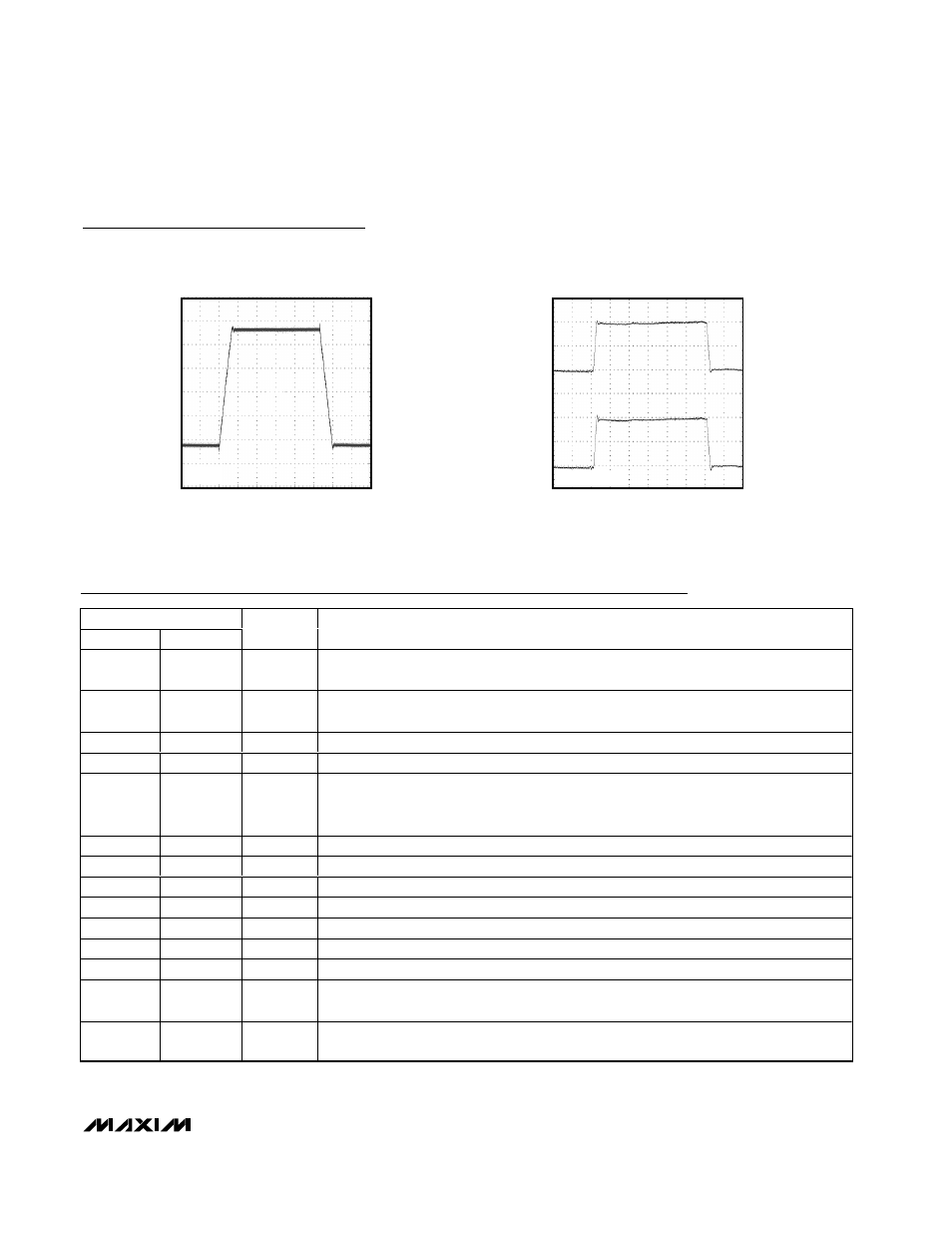
Typical Operating Characteristics (continued)
(V
IN
= 3.3V, V
MAIN
= 8V, f
OSC
= 1.2MHz, T
A
= +25°C, unless otherwise noted.)
OPERATIONAL AMPLIFIER
SMALL-SIGNAL STEP RESPONSE
MAX1542 toc24
200ns/div
POS_
50mV/div
AC-COUPLED
OUT_
50mV/div
AC-COUPLED
V
SUP
= 8V, A
V
= 1
CH2 + OVER
6.234%
CH2 - OVER
2.352%
OPERATIONAL AMPLIFIER
LARGE-SIGNAL STEP RESPONSE
MAX1542 toc23
1
µs/div
V
OUT_
1V/div
CHI AMPL
4.86V
CHI + OVER
4.970%
A
V
= 1
Pin Description
PIN
MAX1542
MAX1543
NAME
FUNCTION
1
1
COM
Internal High-Voltage MOSFET Switch Common Terminal. Do not allow the voltage on
COM to exceed V
SRC
.
2
2
SRC
Switch Input. Source of the internal high-voltage P-channel MOSFET. Bypass SRC to
PGND with a minimum of 0.1µF close to the pins.
3, 15, 20
—
N.C.
No Connection. Not internally connected.
—
3
I.C.
Internal Connection. Make no connection to this pin.
4
4
PGND
Power Ground. PGND is the source of the main boost N-channel power MOSFET. Connect
PGND to the output capacitor ground terminals through a short, wide PC board trace.
Connect to analog ground (AGND) underneath the IC.
5
5
AGND
Analog Ground. Connect to power ground (PGND) underneath the IC.
6
6
POS1
Operational Amplifier 1 Noninverting Input
7
7
NEG1
Operational Amplifier 1 Inverting Input
8
8
OUT1
Operational Amplifier 1 Output
9
9
OUT2
Operational Amplifier 2 Output
10
10
NEG2
Operational Amplifier 2 Inverting Input
11
11
POS2
Operational Amplifier 2 Noninverting Input
12
12
SUP
Operational Amplifier Power Input. Positive supply rail for the OUT1 and OUT2 amplifiers.
Typically connected to V
MAIN
. Bypass SUP to AGND with a 0.1µF capacitor.
13
13
LX
Power MOSFET N-Channel Drain and Switching Node. Connect the inductor and catch
diode to LX and minimize the trace area for lowest EMI.