Rainbow Electronics MAX1543 User Manual
Page 17
MAX1542/MAX1543
TFT LCD DC-to-DC Converter with
Operational Amplifiers
______________________________________________________________________________________
17
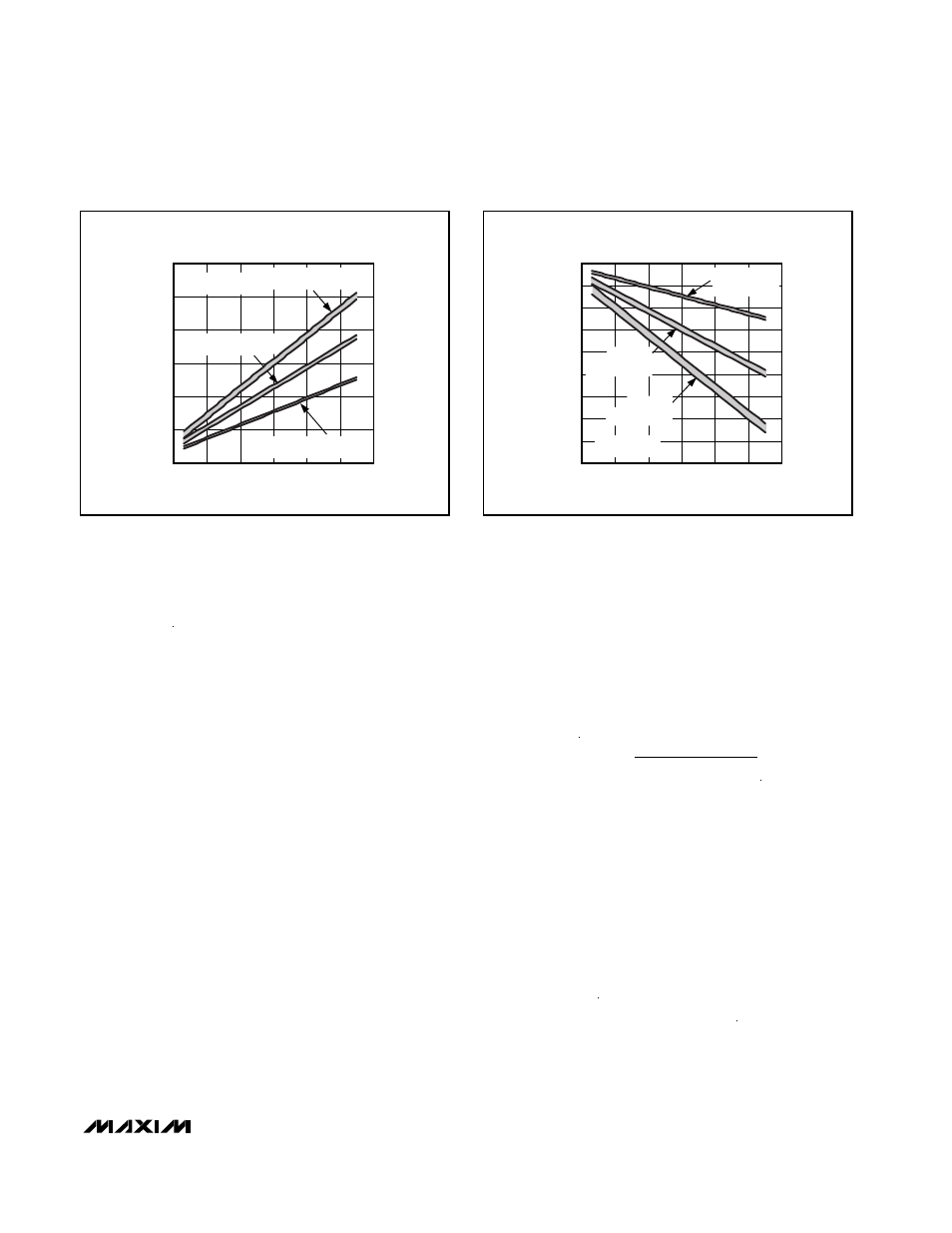
negative charge-pump output voltages for a given
V
MAIN
for one-, two-, and three-stage charge pumps,
based on the following equations:
where G_ON is the positive charge-pump output volt-
age, G_OFF is the negative charge-pump output volt-
age, n is the number of charge-pump stages, and V
D
is
the voltage drop across each diode.
V
D
is the forward voltage drop of the charge-pump
diodes.
Flying Capacitors
Increasing the flying capacitor (C3, C4, and C5) value
increases the output current capability. Increasing the
capacitance indefinitely has a negligible effect on out-
put current capability because the internal switch resis-
tance and the diode impedance limit the source
impedance. A 0.1µF ceramic capacitor works well in
most low-current applications. The flying capacitor’s
voltage rating must exceed the following:
V
CX
> n
✕
V
MAIN
Where n is the stage number in which the flying capaci-
tor appears, and V
MAIN
is the main output voltage. For
example, the two-stage positive charge pump in the
Typical Application Circuits (Figures 1 and 2) where
V
MAIN
= 8V contains two flying capacitors. The flying
capacitor in the first stage (C5) requires a voltage rat-
ing greater than 8V. The flying capacitor in the second
stage (C4) requires a voltage rating greater than 16V.
Charge-Pump Output Capacitor
Increasing the output capacitance or decreasing the
ESR reduces the output ripple voltage and the peak-to-
peak transient voltage. With ceramic capacitors, the
output voltage ripple is dominated by the capacitance
value. Use the following equation to approximate the
required capacitor value:
where V
RIPPLE
is the acceptable peak-to-peak output-
voltage ripple.
Charge-Pump Rectifier Diodes
To maximize the available output voltage, use Schottky
diodes with a current rating equal to or greater than two
times the average charge-pump input current. If the
loaded charge-pump output voltage is greater than
required, some or all of the Schottky diodes can be
replaced with low-cost silicon switching diodes with an
equivalent current rating. The charge-pump input cur-
rent is:
where n is the number of charge-pump stages.
I
I
n
CP IN
CP OUT
_
_
=
×
C
I
F
V
OUT
LOAD
OSC
RIPPLE
≥
Ч
Ч
2
G ON
V
n V
V
G OFF
n V
V
MAIN
MAIN
D
MAIN
D
_
(
)
_
(
)
=
+
−
= −
−
POSITIVE CHARGE-PUMP
OUTPUT VOLTAGE vs. V
MAIN
V
MAIN
(V)
G_ON (V)
12
10
8
6
4
10
20
30
40
50
60
0
2
14
2-STAGE CHARGE-PUMP
3-STAGE CHARGE-PUMP
V
D
= 0.3V TO 1V
1-STAGE CHARGE-PUMP
Figure 5. Positive Charge-Pump Output Voltage vs. V
MAIN
NEGATIVE CHARGE-PUMP
OUTPUT VOLTAGE vs. V
MAIN
V
MAIN
(V)
G_OFF (V)
12
10
8
6
4
-40
-35
-30
-25
-20
-15
-10
-5
-0
-45
2
14
1-STAGE
CHARGE-PUMP
2-STAGE
CHARGE-PUMP
3-STAGE
CHARGE-PUMP
V
D
= 0.3V TO 1V
Figure 6. Negative Charge-Pump Output Voltage vs. V
MAIN