Table 1. component list, Table 2. component suppliers – Rainbow Electronics MAX1543 User Manual
Page 11
MAX1542/MAX1543
TFT LCD DC-to-DC Converter with
Operational Amplifiers
______________________________________________________________________________________
11
The regulator controls the output voltage and the power
delivered to the outputs by modulating the duty cycle
(D) of the power MOSFET in each switching cycle. The
duty cycle of the MOSFET is approximated by:
The device regulates the output voltage through a com-
bination of an error amplifier, two comparators, and
several signal generators (Figure 3). The error amplifier
compares the signal at FB to 1.24V and varies the
COMP output. The voltage at COMP determines the
current trip point each time the internal MOSFET turns
on. As the load varies, the error amplifier sources or
sinks current to the COMP output accordingly to pro-
duce the inductor peak current necessary to service
the load. To maintain stability at high duty cycles, a
slope compensation signal is summed with the current-
sense signal.
Operational Amplifiers
The MAX1542/MAX1543 include two operational ampli-
fiers that are typically used to drive the LCD backplane
VCOM and/or the gamma correction divider string. The
operational amplifiers feature ±150mA output short-cir-
cuit current, 7.5V/µs slew rate, and 12MHz bandwidth.
The rail-to-rail inputs and outputs maximize flexibility.
Short-Circuit Current Limit
The MAX1542/MAX1543 operational amplifiers limit
short-circuit current to ±150mA if the output is directly
shorted to SUP or AGND. In such a condition, the junc-
tion temperature of the IC rises until it reaches the ther-
mal shutdown threshold, typically +160°C. Once it
reaches this threshold, the IC shuts down and remains
inactive until IN falls below V
UVLO
.
Driving Pure Capacitive Loads
The operational amplifiers are typically used to drive
the LCD backplane (VCOM) or the gamma correction
divider string. The LCD backplane consists of a distrib-
uted series capacitance and resistance, a load easily
driven by the operational amplifiers. However, if the
operational amplifiers are used in an application with a
pure capacitive load, steps must be taken to ensure
stable operation.
As the operational amplifier’s capacitive load increases,
the amplifier bandwidth decreases and gain peaking
increases. A small 5
Ω to 50Ω resistance placed between
OUT_ and the capacitive load reduces peaking but
reduces the amplifier gain. An alternative method of
reducing peaking is the use of a snubber circuit. A 150
Ω
and 10nF (typ) shunt load, or snubber, does not continu-
ously load the output or reduce amplifier gain.
D
V
V
V
MAIN
IN
MAIN
≈
−
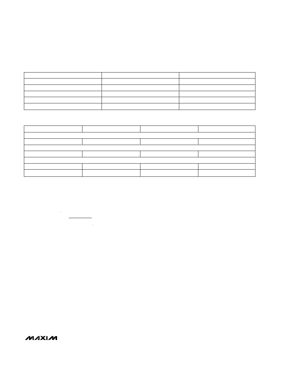
DESIGNATION
DESCRIPTION
PART
C1
10µF ±10%, 6.3V X5R ceramic capacitor
TDK C3216X5R0J106K
C8, C9
4.7µF ±10%, 10V X5R ceramic capacitors
TDK C3225X5R1A475K
D1
1A, 30V Schottky diode
Toshiba CRS02
D2, D3, D4
200mA, 100V dual ultra-fast diodes
Fairchild MMBD4148SE
L1
4.7µH, 1.3A inductor
Sumida CLS5D11HP-4R7
Table 1. Component List
SUPPLIER
PHONE
FAX
WEBSITE
Inductors
Sumida USA
847-956-0666
847-956-0702
www.sumida.com
Capacitors
TDK
847-803-6100
847-803-6296
www.component.tdk.com
Diodes
Fairchild
888-522-5372
408-822-2104
www.fairchildsemi.com
Toshiba
949-455-2000
949-859-3963
www.toshiba.com/taec/
Table 2. Component Suppliers