Rainbow Electronics MAX1543 User Manual
Page 15
MAX1542/MAX1543
TFT LCD DC-to-DC Converter with
Operational Amplifiers
______________________________________________________________________________________
15
values also require more energy storage and more
turns of wire, which increase physical size and can
increase I
2
R losses in the inductor. Low inductance val-
ues decrease the physical size but increase the current
ripple and peak current. Finding the best inductor
involves choosing the best compromise between circuit
efficiency, inductor size, and cost.
The equations used here include a constant, LIR, which
is the ratio of the inductor peak-to-peak ripple current to
the average DC inductor current at the full output cur-
rent. The best trade-off between inductor size and cir-
cuit efficiency for step-up converters generally has an
LIR between 0.3 and 0.5. However, depending on the
AC characteristics of the inductor core material and
ratio of inductor resistance to other power path resis-
tances, the best LIR can shift up or down. If the inductor
resistance is relatively high, more ripple can be accept-
ed to reduce the number of turns required and increase
the wire diameter. If the inductor resistance is relatively
low, increasing inductance to lower the peak current
can decrease losses throughout the power path. If
extremely thin, high-resistance inductors are used, as is
common for LCD panel applications, the best LIR can
increase to between 0.5 and 1.0.
Once a physical inductor is chosen, higher and lower
values of that inductor should be evaluated for efficien-
cy improvements in typical operating regions.
Calculate the approximate inductor value using the typ-
ical input voltage (V
IN
), the maximum output current
(I
MAIN(MAX)
), the expected efficiency (
η
TYP
) taken from
an appropriate curve in the Typical Operating
Characteristics, and an estimate for LIR based on the
above paragraphs:
Choose an available inductor value from an appropriate
inductor family. Calculate the maximum DC input cur-
rent at the minimum input voltage V
IN(MIN)
using con-
servation of energy and the expected efficiency at that
L
V
x
x V
V
V
x LIR x I
x f
IN
TYP
MAIN
IN
MAIN
MAIN MAX
OSC
(
) /
(
)
(
)
≅
−
2
2
η
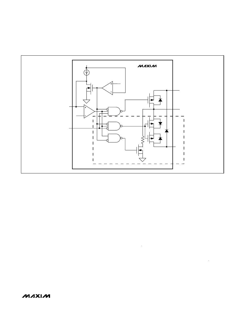
5
µA
Q3
N
SRC
COM
DRN
N
REF
DEL
IN
2.5V
CTL
Q1
Q2
P
1k
Ω
MAX1543 ONLY
P
P
MAX1542
MAX1543
Figure 4. Switch Control