Rainbow Electronics MAX1543 User Manual
Page 12

MAX1542/MAX1543
TFT LCD DC-to-DC Converter with
Operational Amplifiers
12
______________________________________________________________________________________
Delay Control Circuit
A capacitor from DEL to AGND selects the switch control
block supply startup delay. After the input voltage
exceeds V
UVLO
, a 5µA current source charges C
DEL
.
Once the capacitor voltage exceeds the turn-on thresh-
old (1.24V) COM can be connected to SRC, depending
on the state of CTL. Before startup and when IN is less
than V
UVLO
, DEL is internally connected to AGND to dis-
charge C
DEL
. Select C
DEL
using the following equation:
MAX1542 Control Block Switch
The switch control input (CTL) is not activated until
V
DEL
exceeds the turn-on voltage (1.24V) and the input
voltage (V
IN
) exceeds V
UVLO
(2.5V). Once activated,
CTL controls the P-channel MOSFET, between COM
and SRC. A high at CTL turns on Q1 between SRC and
COM, and a low at CTL turns Q1 off (Figure 4).
MAX1543 Control Block Switch
The switch control input (CTL) is not activated until the
input voltage (V
IN
) exceeds V
UVLO
(2.5V) and V
DEL
exceeds the turn-on voltage (1.24V). During UVLO or
when DEL is below the turn-on threshold, COM is
pulled low to PGND through Q3 and a 1k
Ω resistance.
Once activated, CTL controls the COM MOSFETs,
switching COM between SRC and DRN. A high at CTL
turns on Q1 and disables Q2. A low at CTL turns on Q2
and turns off Q1 (Figure 4).
Undervoltage Lockout (UVLO)
The UVLO comparator of the MAX1542/MAX1543 com-
pares the input voltage at IN with the UVLO threshold
C
DELAY TIME
A
V
DEL
=
×
(
)
.
5
1 24
µ
LX
IN
AGND
PGND
DEL
CTL
COM
SRC
COMP
POS2
OUT2
POS1
OUT1
NEG1
SUP
FB
D1
V
MAIN
+8V AT 250mA
TO VCOM
BACKPLANE
D2
D3
D4
-7V AT 20mA
G_OFF
NEG2
G_ON
+22V AT 20mA
MAX1542
R8
100k
Ω
C11
220pF
C10
33nF
V
IN
2.6V TO 5.5V
C1
10
µF
L1
4.7
µF
C2
0.1
µF
C3
0.1
µF
C4
0.1
µF
C5
0.1
µF
C6
0.1
µF
C8
4.7
µF
R1
75k
Ω
C9
4.7
µF
C7
0.1
µF
R5
40k
Ω
R6
40k
Ω
R2
13.7k
Ω
R3
40k
Ω
R4
40k
Ω
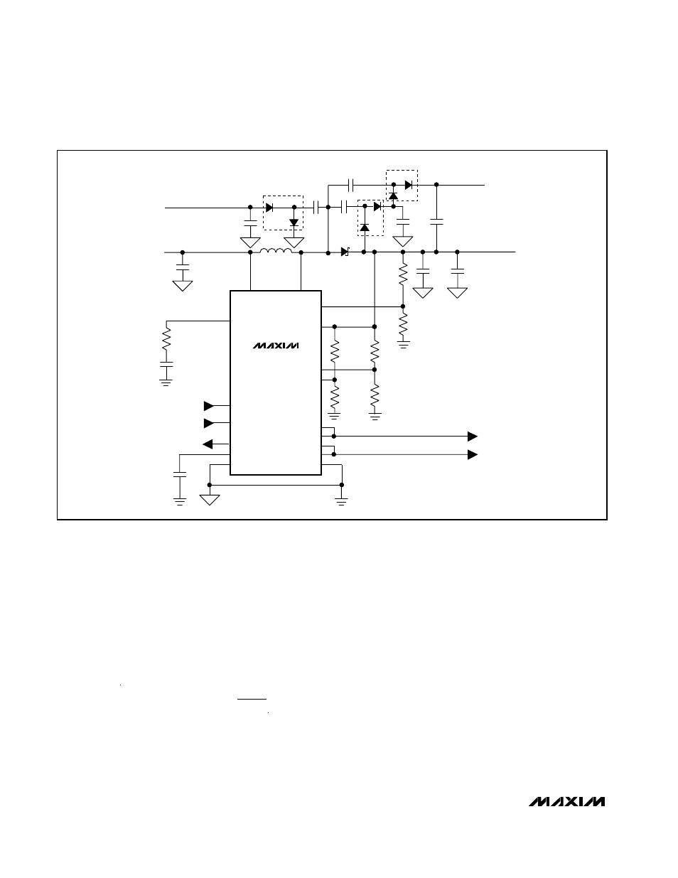
Figure 1. MAX1542 Typical Application Circuit
