Timing characteristics (continued) – Rainbow Electronics MAX1400 User Manual
Page 8
MAX1400
+5V, 18-Bit, Low-Power, Multichannel,
Oversampling (Sigma-Delta) ADC
8
_______________________________________________________________________________________
TIMING CHARACTERISTICS (continued)
(V+ = +5V ±5%, V
DD
= +2.7V to +5.25V, AGND = DGND, f
CLKIN
= 2.4576MHz; input logic 0 = 0V; logic 1 = V
DD
, T
A
= T
MIN
to T
MAX
,
unless otherwise noted.) (Notes 19, 20, 21)
Note 19:
All input signals are specified with t
r
= t
f
= 5ns (10% to 90% of V
DD
).
Note 20:
See Figure 4.
Note 21:
Timings shown in tables are for the case where SCLK idles high between accesses. The part may also be used with the
SCLK idling low between accesses, provided CS is toggled. In this case SCLK in the timing diagrams should be inverted
and the terms “SCLK Falling Edge” and “SCLK Rising Edge” exchanged in the specification tables. If CS is permanently
tied low, the part should only be operated with SCLK idling high between accesses.
Note 22:
CLKIN duty cycle range is 45% to 55%. CLKIN must be supplied whenever the MAX1400 is not in standby mode. If no
clock is present, the device can draw higher current than specified.
Note 23:
The MAX1400 is production tested with f
CLKIN
at 2.5MHz (1MHz for some I
DD
tests).
Note 24:
Measured with the load circuit of Figure 1 and defined as the time required for the output to cross the V
OL
or V
OH
limits.
Note 25:
For read operations, SCLK active edge is falling edge of SCLK.
Note 26:
Derived from the time taken by the data output to change 0.5V when loaded with the circuit of Figure 1. The number is then
extrapolated back to remove effects of charging or discharging the 50pF capacitor. This ensures that the times quoted in
the timing characteristics are true bus-relinquish times and are independent of external bus loading capacitances.
Note 27:
INT returns high after the first read after an output update. The same data can be read again while INT is high, but be
careful not to allow subsequent reads to occur close to the next output update.
CS Rising Edge to SCLK Rising
Edge Hold Time
t
18
0
ns
SCLK High Pulse Width
t
16
100
ns
SCLK Low Pulse Width
t
17
100
ns
Data Valid to SCLK Rising Edge
Hold Time
t
15
0
ns
PARAMETER
SYMBOL
MIN
TYP
MAX
UNITS
CS Falling Edge to SCLK Falling
Edge Setup Time
t
13
30
ns
Data Valid to SCLK Rising Edge
Setup Time
t
14
30
ns
SCLK Setup to Falling Edge CS
t
12
30
ns
CONDITIONS
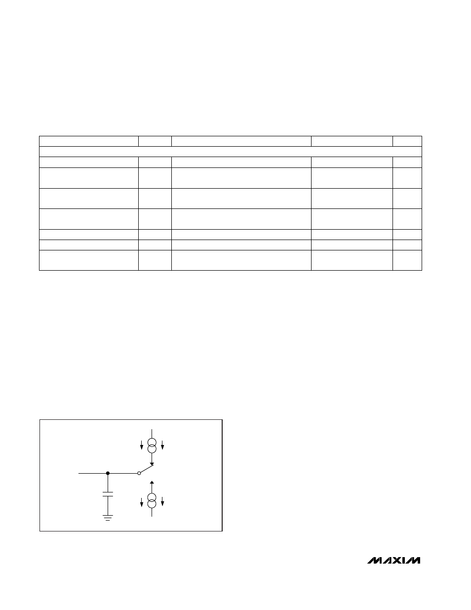
SERIAL-INTERFACE WRITE OPERATION
800
µ
A
at V
DD
= +5V
100
µ
A
at V
DD
= +3.3V
100
µ
A
at V
DD
= +3.3V
TO
OUTPUT
PIN
50pF
200
µ
A
at V
DD
= +5V
Figure 1. Load Circuit for Bus Relinquish Time and V
OL
and
V
OH
Levels