Rainbow Electronics MAX1400 User Manual
Page 16
First Bit (MSB)
(LSB)
MAX1400
+5V, 18-Bit, Low-Power, Multichannel,
Oversampling (Sigma-Delta) ADC
16
______________________________________________________________________________________
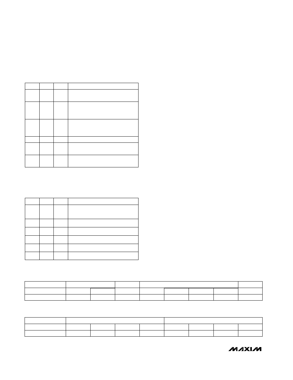
Special Function Register (Write-Only)
MDOUT:
(Default = 0) Modulator Out Bit. MDOUT = 0
enables data readout on the DOUT pin, the normal con-
dition for the serial interface. MDOUT = 1 changes the
function of the DOUT and INT pins, providing raw, sin-
gle-bit modulator output instead of the normal serial-
data interface output. This allows custom filtering
directly on the modulator output, without going through
the on-chip digital filter. The INT pin provides a clock to
indicate when the modulator data at DOUT should be
sampled (falling edge of INT). Note that in this mode,
the on-chip digital filter continues to operate normally.
When MDOUT is returned to 0, valid data may be
accessed through the normal serial-interface read
operation.
FULLPD:
(Default = 0) Complete Power-Down Bit.
FULLPD = 1 forces the part into a complete power-
down condition, which includes the clock oscillator. The
serial interface continues to operate. The part requires a
hardware reset to recover correctly from this condition.
Note:
Changing the reserved bits in the special-func-
tion register from the default status of all 0s will select
one of the reserved modes and the part will not operate
as expected. This register is a write-only register.
However, in the event that this register is mistakenly
read, clock 24 bits of data out of the part to restore it to
the normal interface-idle state.
Transfer-Function Registers
The three transfer-function registers control the method
used to map the input voltage to the output codes. All
of the registers have the same format. The mapping of
control registers to associated channels depends on
the mode of operation and is affected by the state of
M1, M0, DIFF, and SCAN (Tables 8, 9, and 10).
Table 4. SCAN Mode Scanning
Sequences (SCAN = 1)
Table 5. Available Input Channels
(SCAN = 0)
Note:
All other combinations reserved.
First Bit (MSB)
(LSB)
AVAILABLE CHANNELS
DIFF
1
CALOFF
1
CALGAIN
0
1
1
0
0
0
AIN1–AIN6, AIN2–AIN6,
AIN3–AIN6, AIN4–AIN6
CALGAIN
1
AIN1–AIN2, AIN3–AIN4, AIN5–AIN6
0
0
0
1
0
CALOFF
1
0
M0
0
M1
0
FUNCTION
0
RESERVED BITS
0
0
0
0
Name
FULLPD
0
0
0
MDOUT
0
RESERVED BITS
Defaults
0
0
0
0
0
FUNCTION
0
U/B
0
0
G0
D1
0
0
D2
0
OFFSET CORRECTION
Name
D0
PGA GAIN CONTROL
G1
Defaults
0
0
D3
G2
SEQUENCE
DIFF
1
AIN1–AIN2, AIN3–AIN4,
AIN5–AIN6, CALOFF, CALGAIN
1
AIN1–AIN2, AIN3–AIN4,
AIN5–AIN6, CALOFF, CALGAIN
0
1
1
0
0
0
AIN1–AIN6, AIN2–AIN6, AIN3–AIN6,
AIN4–AIN6, AIN5–AIN6
AIN1–AIN6, AIN2–AIN6,
AIN3–AIN6, AIN4–AIN6,
AIN5–AIN6, CALOFF, CALGAIN
1
AIN1–AIN2, AIN3–AIN4, AIN5–AIN6
0
0
0
1
0
AIN1–AIN6, AIN2–AIN6, AIN3–AIN6,
AIN4–AIN6, AIN5–AIN6, CALOFF,
CALGAIN
1
0
M0
0
M1
0
Special Function Register (Write-Only)
Transfer-Function Register