Timing characteristics – Rainbow Electronics MAX1400 User Manual
Page 7
MAX1400
+5V, 18-Bit, Low-Power, Multichannel,
Oversampling (Sigma-Delta) ADC
_______________________________________________________________________________________
7
Note 16:
Measured at DC in the selected passband. PSR at 50Hz will exceed 120dB with filter notches of 25Hz or 50Hz and FAST
bit = 0. PSR at 60Hz will exceed 120dB with filter notches of 20Hz or 60Hz and FAST bit = 0.
Note 17:
PSR depends on gain. For a gain of +1V/V, PSR is 70dB typical. For a gain of +2V/V, PSR is 75dB typical. For a gain of
+4V/V, PSR is 80dB typical. For gains of +8V/V to +128V/V, PSR is 85dB typical.
Note 18:
Standby power-dissipation and current specifications are valid only with CLKIN driven by an external clock and with the
external clock stopped. If the clock continues to run in standby mode, the power dissipation will be considerably higher.
When used with a resonator or crystal between CLKIN and CLKOUT, the actual power dissipation and I
DD
in standby
mode will depend on the resonator or crystal type.
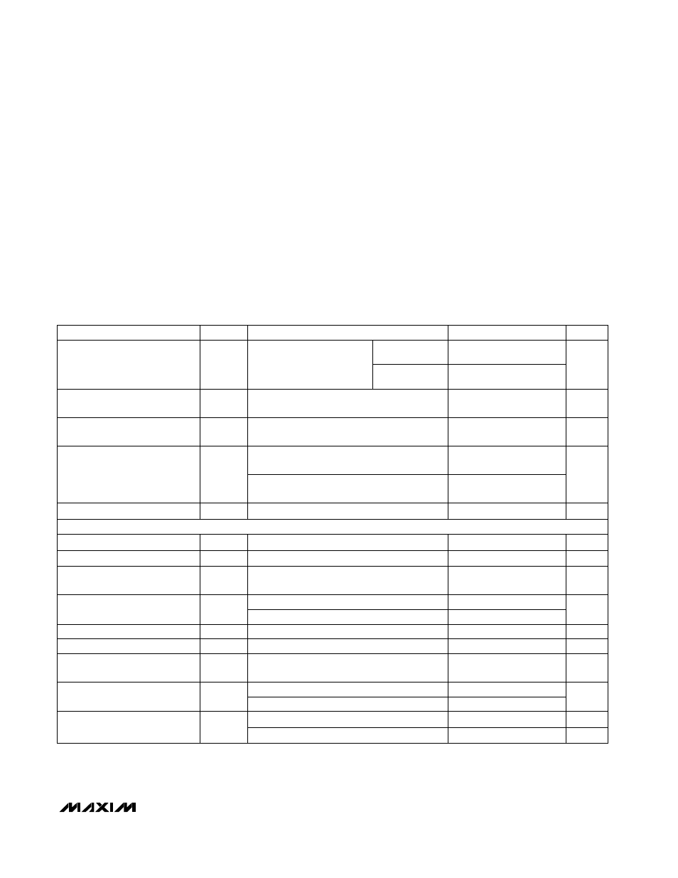
TIMING CHARACTERISTICS
(V+ = +5V ±5%, V
DD
= +2.7V to +5.25V, AGND = DGND, f
CLKIN
= 2.4576MHz; input logic 0 = 0V; logic 1 = V
DD
, T
A
= T
MIN
to T
MAX
,
unless otherwise noted.) (Notes 19, 20, 21)
0
100
V
DD
= 3.3V
V
DD
= 5V
V
DD
= 3.3V
V
DD
= 5V
Bus Relinquish Time After SCLK
Rising Edge (Note 26)
t
10
10
100
ns
SCLK Falling Edge to Data Valid
Delay (Notes 24, 25)
t
6
0
80
ns
INT High Time
t
INT
560 / N
·
t
CLKIN
ns
X2CLK = 1, N = 2
(2
·
MF1 + MF0)
X2CLK = 1
X2CLK = 0
SCLK Setup to Falling Edge CS
t
4
30
ns
SCLK Low Pulse Width
t
8
100
ns
10
70
100
ns
V
DD
= 5V
CS Rising Edge to SCLK Rising
Edge Hold Time (Note 21)
t
9
0
ns
SCLK High Pulse Width
t
7
100
ns
CS Falling Edge to SCLK Falling
Edge Setup Time
t
5
30
ns
280 / N
·
t
CLKIN
INT to CS Setup Time (Note 8)
t
3
X2CLK = 0, N = 2
(2
·
MF1 + MF0)
0
ns
RESET Pulse Width Low
t
2
100
ns
Master Clock Input Low Time
f
CLKIN LO
0.4
·
t
CLKIN
ns
t
CLKIN
= 1 / f
CLKIN
, X2CLK = 0
Master Clock Input High Time
f
CLKIN HI
0.4
·
t
CLKIN
ns
t
CLKIN
= 1 / f
CLKIN
, X2CLK = 0
Master Clock Frequency
f
CLKIN
0.8
5.0
MHz
Crystal oscillator or clock
externally supplied for
specified performance
(Notes 22, 23)
PARAMETER
SYMBOL
MIN
TYP
MAX
UNITS
0.4
2.5
CONDITIONS
SCLK Rising Edge to INT High
(Note 27)
t
11
200
ns
V
DD
= 3.3V
SERIAL-INTERFACE READ OPERATION